-


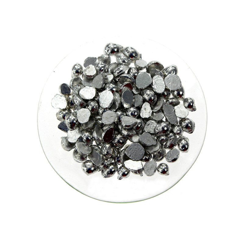
- High Purity: Cadmium pellets are typically available with purity levels of 99.9% or higher, ensuring the creation of defect-free, high-quality thin films.
- Low Melting Point: Cadmium has a relatively low melting point, making it easy to evaporate in deposition processes.
- Electrical Properties: Cadmium’s electrical conductivity and ability to form alloys make it valuable in semiconductor and electronic applications.
- Optical Properties: Cadmium thin films are used in optical devices due to their favorable reflective and refractive properties in certain wavelengths, especially in the IR and visible regions.
- Corrosion Resistance: Cadmium coatings offer protection from corrosion, especially in aerospace and marine equipment, by serving as a sacrificial layer to protect underlying materials.
-


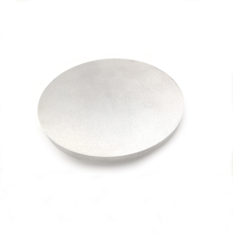
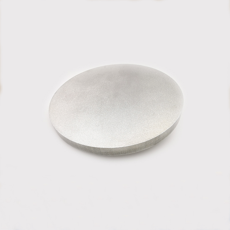
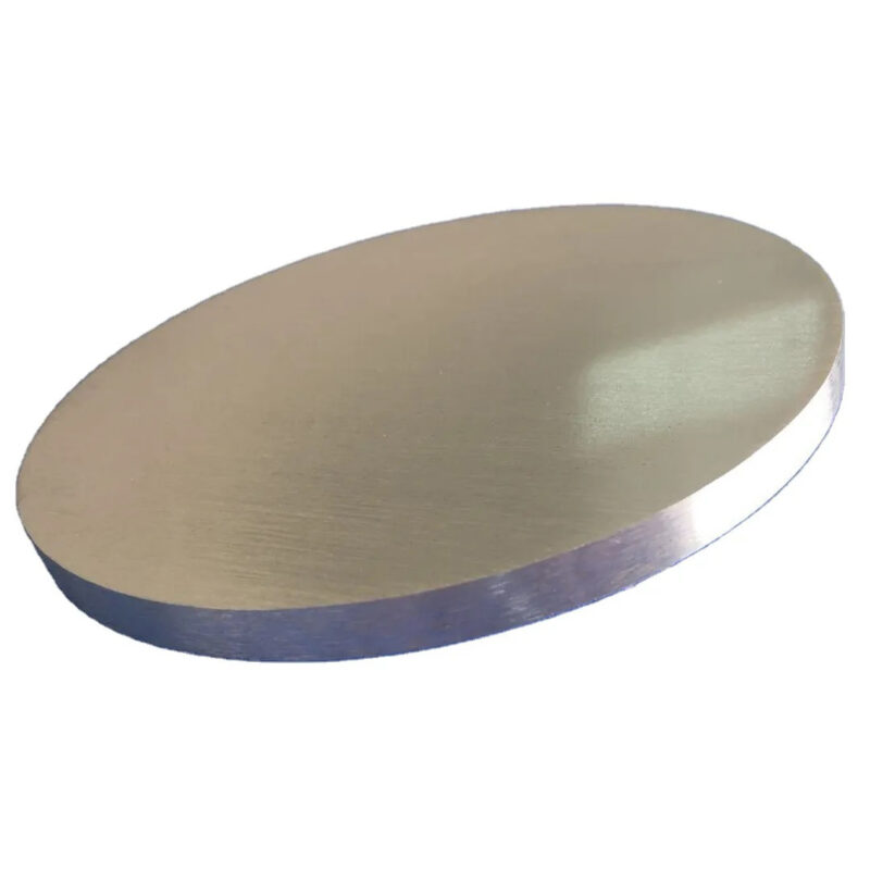
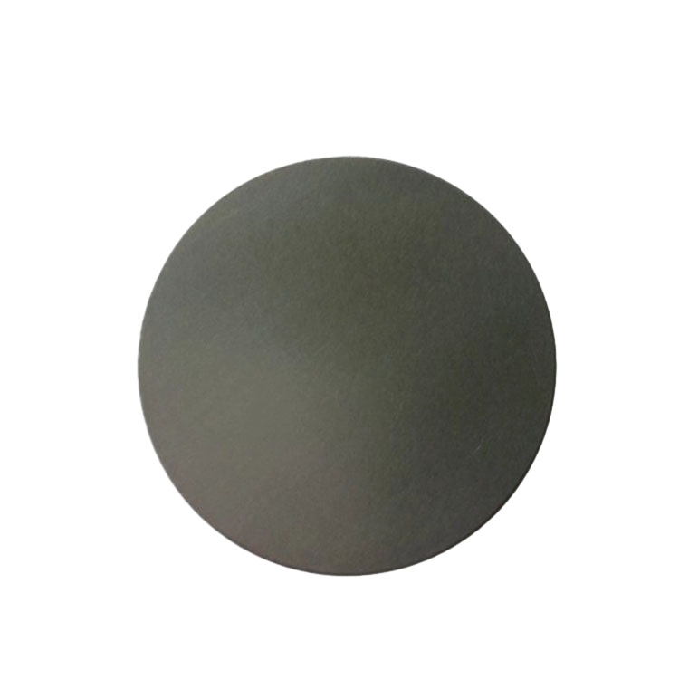
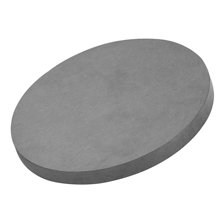
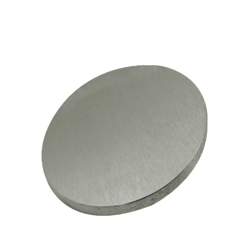
- Shapes Available: Circular (disc), rectangular, and custom-designed targets.
- Diameter Range: Custom sizes available.
- Thickness: Varies depending on application requirements.
- Surface Finish: Fine-polished to ensure uniform film deposition.
- Backing Plate: Available with or without bonding to enhance thermal and mechanical stability.
-

- High Electrical Conductivity: CdO is known for its good electrical conductivity, making it an excellent material for use in electronic and optoelectronic devices.
- Optical Transparency: CdO films offer transparency in the visible light spectrum, making them ideal for TCO applications.
- Good Chemical Stability: CdO targets provide stable films that resist degradation in various environmental conditions.
- Infrared Absorption: CdO’s strong absorption properties in the infrared range are advantageous for applications in IR optics and detectors.
-


- Direct Bandgap Semiconductor: CdS has a direct bandgap (~2.42 eV), making it an excellent material for optoelectronic applications requiring high-efficiency light absorption and emission.
- High Transparency: CdS exhibits high transparency in the visible spectrum, making it an ideal candidate for window layers in photovoltaic devices.
- Stable and Efficient: CdS is a stable semiconductor with efficient electron-hole pair generation, which enhances the performance of solar cells and optoelectronic devices.
- Low-cost Semiconductor: Compared to other semiconductors, CdS offers a cost-effective solution for large-scale production in photovoltaics and other electronics.
-


- Optical Properties: CdSe exhibits strong light absorption in the visible and infrared spectrum, making it an ideal material for optoelectronic applications.
- Electronic Properties: With a direct bandgap of approximately 1.7 eV (which can be tuned depending on particle size and synthesis methods), CdSe offers high photoresponsivity and efficient charge carrier transport.
- Thermal Stability: CdSe maintains good chemical and structural stability within a specific temperature range.
- Crystal Structure: It exists in either a cubic (zinc blende) or hexagonal (wurtzite) crystalline phase, each with distinct electronic and optical characteristics.
-

- Direct Bandgap Semiconductor: CdSe has a direct bandgap (~1.74 eV), making it ideal for optoelectronic applications such as light-emitting devices, lasers, and photovoltaics.
- High Absorption Coefficient: CdSe exhibits a high absorption coefficient in the visible range, making it suitable for applications in solar cells and photodetectors.
- Quantum Dot Applications: CdSe is widely used in quantum dots, offering tunable emission properties based on the size of the particles, enabling use in next-generation displays and medical imaging.
- Wide Range of Optical and Electronic Properties: CdSe offers tunable optical and electronic properties, making it useful across a wide range of applications from sensors to light-emitting devices.
-

- Excellent Photovoltaic Properties: TeCd, especially CdTe, is widely used in thin-film solar cells due to its excellent light absorption and efficient energy conversion.
- Infrared Sensitivity: TeCd thin films exhibit high sensitivity to infrared light, making them suitable for infrared detectors and thermal imaging devices.
- Stable Thin Films: TeCd films are chemically stable and durable, ensuring long-term performance in harsh environmental conditions.
- Efficient Energy Conversion: TeCd materials offer high energy conversion efficiency, particularly in solar and thermoelectric applications, providing reliable performance in energy devices.
