Showing 1–12 of 31 results
-

- High purity (≥99.99%).
- Exceptional infrared transmission properties.
- Semiconductor material with high thermal and chemical stability.
- Suitable for thin-film deposition techniques like PVD and CVD.
- Custom sizes and shapes available.
-

- Semiconducting Properties: Bi₂S₃ is a narrow-band-gap semiconductor, which makes it efficient for applications requiring light absorption, such as solar cells and photodetectors.
- High Absorptivity: The material has high light absorption in the visible and near-infrared ranges, making it ideal for optoelectronic applications.
- Good Thermal Stability: Bi₂S₃ thin films are thermally stable, making them suitable for high-temperature applications such as thermoelectric devices.
- Non-toxic Alternative: Bismuth-based materials, including Bi₂S₃, are considered less toxic compared to heavy metal-based semiconductors, offering a more environmentally friendly option for various applications.
-

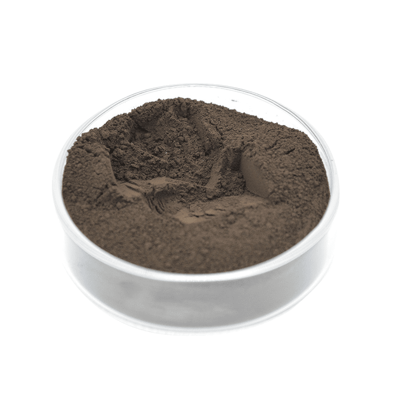
- High Purity: Available with ≥99.9% purity for precise applications.
- Exceptional Optical Properties: Narrow bandgap and strong absorption in visible and infrared spectra.
- Thermoelectric Efficiency: High thermoelectric performance for energy conversion applications.
- Chemical Stability: Resistant to oxidation and environmental degradation.
- Customizable Particle Sizes: Available in nano and micro scales to suit different requirements.
- Eco-friendly: Non-toxic and environmentally friendly material.
-

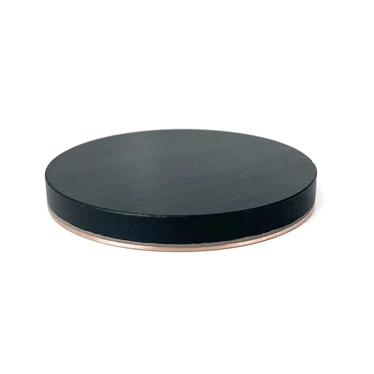
- High Conductivity: Bi₂S₃ films exhibit good electrical conductivity, making them ideal for use in electronic applications.
- Thermoelectric Efficiency: Known for its high thermoelectric performance, making it a key material in thermoelectric energy conversion devices.
- Optical Transparency: The material has desirable optical transparency in the visible spectrum, which is advantageous for optoelectronic applications.
- Chemical Stability: Bismuth Sulfide is stable under a wide range of chemical conditions, which ensures longevity and reliability in demanding environments.
- High Purity: Bi₂S₃ sputtering targets are available in high purity, ensuring the production of high-quality thin films with minimal contamination.
-


- Direct Bandgap Semiconductor: CdS has a direct bandgap (~2.42 eV), making it an excellent material for optoelectronic applications requiring high-efficiency light absorption and emission.
- High Transparency: CdS exhibits high transparency in the visible spectrum, making it an ideal candidate for window layers in photovoltaic devices.
- Stable and Efficient: CdS is a stable semiconductor with efficient electron-hole pair generation, which enhances the performance of solar cells and optoelectronic devices.
- Low-cost Semiconductor: Compared to other semiconductors, CdS offers a cost-effective solution for large-scale production in photovoltaics and other electronics.
-


- Semiconductor Properties: Cu₂S has p-type semiconductor properties, making it suitable for various electronic and photovoltaic applications.
- Good Optical Absorption: Cu₂S efficiently absorbs light, especially in the visible and near-infrared regions, making it ideal for solar cell applications.
- High Conductivity: Cu₂S exhibits good electrical conductivity, which is useful in applications that require conductive thin films.
- Thermal and Chemical Stability: Copper(I) Sulfide is thermally stable and resistant to certain chemicals, ensuring durability in harsh environments.
-

- High Optical Absorption: Cu2S exhibits strong absorption in the visible and near-infrared regions, making it effective for light-harvesting devices like solar cells.
- Good Semiconductor Properties: Copper(I) Sulfide has favorable electrical properties that make it a valuable material for semiconductors and related electronic devices.
- Thermal Stability: The material maintains stability at high evaporation temperatures, ensuring high-quality thin films in evaporation processes.
- High Purity: Available in high purity, ensuring minimal contamination and consistent thin film deposition for sensitive applications.
-

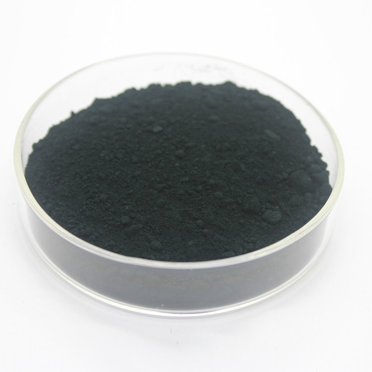
- High Purity: Ensures reliable performance in sensitive applications.
- Semiconducting Properties: Ideal for photovoltaic and electronic devices.
- Thermal Stability: Maintains properties at elevated temperatures.
- Customizable Particle Sizes: Nano and micron-sized powders for specific needs.
- Eco-friendly: Suitable for green energy applications.
- Wide Application Range: Useful in electronics, catalysis, and sensors.
-


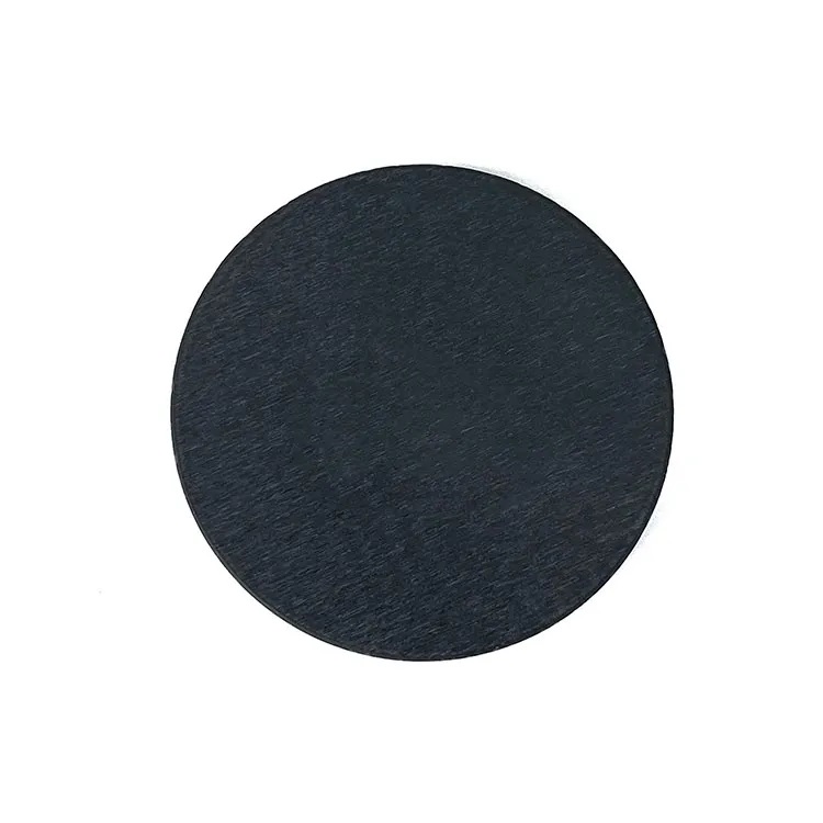
- Semiconductor Properties: CuS is a p-type semiconductor, making it suitable for applications in photovoltaics and semiconductor devices.
- High Absorption: Copper Sulfide has strong light absorption characteristics, especially in the visible spectrum, making it ideal for solar energy applications.
- Customizable: CuS sputtering targets can be customized in terms of size, purity, and bonding options to meet specific deposition requirements.
- High Chemical Stability: CuS is chemically stable, which ensures the longevity and durability of the deposited thin films.
-

- High Purity: Suitable for demanding industrial and research applications.
- Semiconducting Behavior: Ideal for electronic and photovoltaic uses.
- Optical Absorption: Effective for applications requiring light absorption in the infrared spectrum.
- Thermal Stability: Resists degradation at high temperatures.
- Customizable Sizes: Available in nano and micron scales.
- Environmentally Friendly: Supports green energy and eco-conscious applications.
-

- Wide Bandgap: GaS possesses a wide bandgap of about 2.5 eV, making it suitable for UV and visible light applications.
- High Purity: GaS targets are available in high-purity forms to ensure the quality and performance of the deposited films.
- Layered Structure: The layered nature of GaS allows for easy mechanical exfoliation, enabling the production of high-quality monolayers and thin films.
- Thermal Stability: GaS exhibits good thermal stability, maintaining its properties during high-temperature processing.
- Good Electrical Conductivity: GaS is a good electrical conductor, making it valuable in electronic applications.
-

- Semiconducting properties: GeS is a semiconductor with excellent electrical conductivity, ideal for use in electronic and optoelectronic applications.
- Optical performance: The material exhibits specific optical properties that make it suitable for optoelectronic and sensor devices.
- High purity: GeS sputtering targets are available in high purity for optimal thin film quality.
- Customizable: Can be tailored for various applications, with flexibility in composition, size, and target specifications.
