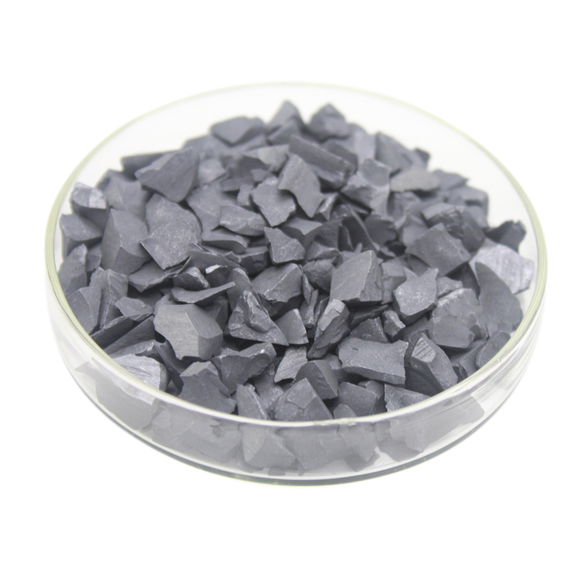
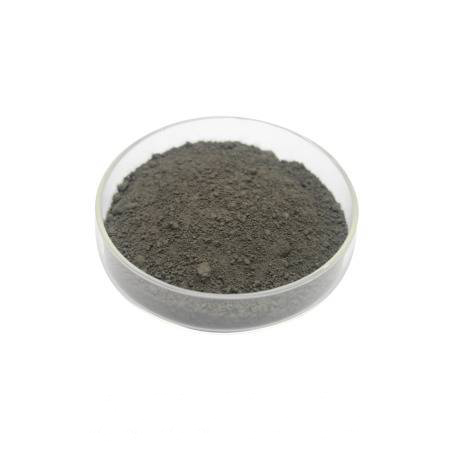
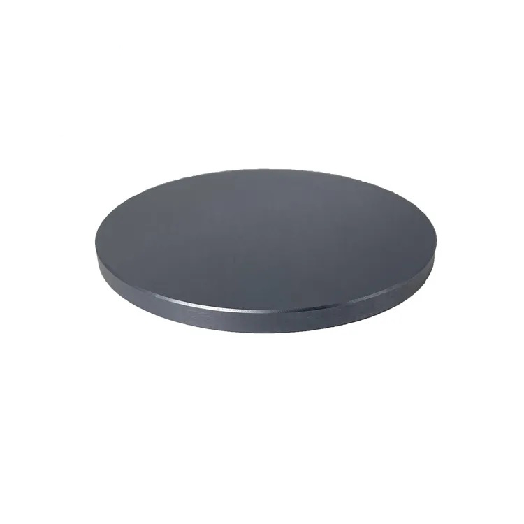
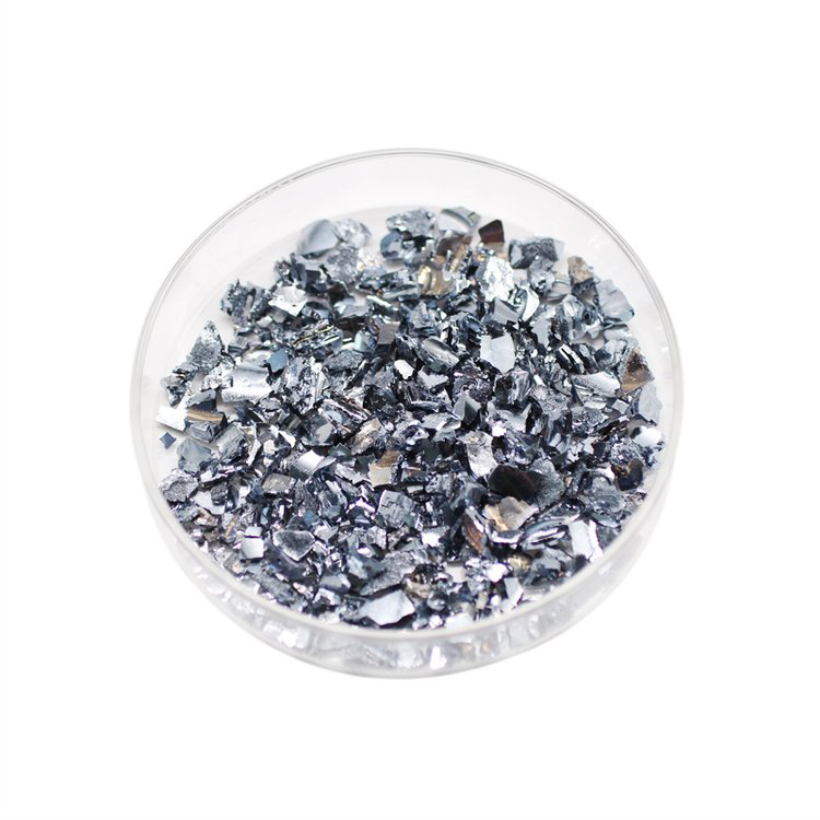
Showing 13–24 of 31 results
-

- High purity (≥99.9%).
- Exceptional semiconducting and optical properties.
- Low toxicity and environmentally friendly.
- Uniform pellet size for consistent deposition.
- Customizable sizes and shapes.
-


- High Optical Transparency: Suitable for applications requiring minimal light absorption.
- Wide Bandgap: Excellent for photovoltaic and semiconductor applications.
- Low Toxicity: Eco-friendly alternative to cadmium-based materials.
- Customizable Specifications: Tailored for specific deposition processes and applications.
- High Purity: Ensures consistent film quality and enhanced device performance.
-


- Layered Structure: MoS₂ has a unique layered structure, allowing for exfoliation into single or few layers, making it ideal for 2D material applications.
- Semiconductor Properties: MoS₂ is a semiconductor with a direct bandgap (~1.8 eV for monolayers), making it suitable for nanoscale transistors and photodetectors.
- Low Friction Coefficient: Its excellent lubrication properties make MoS₂ ideal for coatings that require low friction and high durability, especially in vacuum or extreme conditions.
- Thermal Stability: MoS₂ remains stable at high temperatures, ensuring its effectiveness in harsh environments.
- Corrosion Resistance: MoS₂ provides a protective, corrosion-resistant layer in various applications, extending the life of coated components.
-

- Superior Lubrication: Known for its excellent lubrication properties, particularly in extreme temperature and pressure environments.
- High Wear Resistance: Provides exceptional wear protection and reduces friction in moving parts.
- Thermal Stability: Maintains stability at high temperatures, making it suitable for demanding industrial environments.
- Good Conductivity: Possesses moderate electrical conductivity, making it useful in electrical applications.
- Chemical Resistance: Highly resistant to oxidation and corrosion, making it durable in harsh chemical environments.
- Fine Powder Form: Available in various particle sizes, offering flexibility for different applications.
-


- Layered Structure: MoS2 has a unique layered structure that contributes to its mechanical, electrical, and tribological properties, making it an excellent candidate for advanced coatings and devices.
- Semiconducting Properties: MoS2 is a semiconductor with a direct bandgap in its monolayer form, offering high performance in electronic devices such as transistors and photodetectors.
- Low Friction Coefficient: As a solid lubricant, MoS2 provides a low friction coefficient, making it useful in harsh environments where liquid lubricants are impractical.
- High Thermal and Chemical Stability: MoS2 films exhibit excellent thermal and chemical stability, enabling their use in high-temperature environments and chemically aggressive conditions.
-

- Narrow Bandgap: PbS has a small bandgap (~0.37 eV), allowing it to detect and respond to IR radiation, making it ideal for infrared applications.
- High Infrared Sensitivity: PbS thin films exhibit excellent sensitivity to infrared light, especially in the mid-IR range, enhancing performance in IR detectors and sensors.
- Efficient Light Absorption: PbS absorbs light efficiently, making it a great material for photovoltaic devices and optoelectronic components.
- Good Thermal Stability: PbS films maintain their properties under moderate temperature conditions, suitable for use in thermal and IR-sensitive devices.
- Adaptability to Thin Films: PbS can be easily deposited as a thin film via evaporation, making it suitable for creating highly sensitive IR detectors and optical coatings.
-

- Excellent Light Absorption: Sb2S3 has a high absorption coefficient, especially in the visible and near-IR regions, making it ideal for applications in photovoltaics and infrared detection.
- Semiconducting Properties: Sb2S3 is a direct bandgap semiconductor (~1.7 eV) suitable for energy conversion and electronic devices.
- Layered Structure: The material’s unique crystal structure allows for efficient charge transport and thermal conductivity, which is beneficial for thermoelectric and phase-change applications.
- Thermal Stability: Sb2S3 shows good stability during the deposition process, allowing for high-quality film formation.
- Environmentally Friendly: Sb2S3 is considered an eco-friendly alternative to some toxic or rare materials used in similar applications.
-

- High Optical Absorption: Sb₂S₃ is known for its strong absorption in the visible and near-infrared regions, making it ideal for photovoltaic and optoelectronic applications.
- Environmentally Friendly: Sb₂S₃ is composed of elements that are abundant and less toxic compared to other heavy metals used in similar applications.
- Tunability: The bandgap of Sb₂S₃ can be tuned by modifying deposition parameters, allowing for control over its optical and electronic properties in thin films.
- Thermoelectric Properties: Sb₂S₃ is being explored for its potential to generate electrical energy from thermal gradients, offering promise in energy-harvesting devices.
-

- High purity (≥99.99%).
- Outstanding semiconducting properties with a direct bandgap.
- Suitable for thin-film deposition methods like PVD and CVD.
- Excellent stability under high-temperature and chemical conditions.
- Customizable sizes and packaging options available.
-

- High Purity: SnS with ≥99.9% purity ensures consistent performance.
- Semiconducting Properties: Excellent electronic and optoelectronic behavior.
- Environmentally Friendly: Non-toxic and abundant material suitable for green energy applications.
- Versatility: Applicable across photovoltaics, electronics, and coatings.
- Customizable: Available in various particle sizes to suit different applications.
- Thermal Stability: Performs well in high-temperature environments.
-

- High purity (≥99.99%).
- Semiconductor material with strong optical and electronic properties.
- Excellent performance in thin-film deposition techniques like PVD and CVD.
- Stable under high-temperature and chemical conditions.
- Custom sizes and packaging available.
-

- High Purity: Tin Disulfide with purity levels of ≥99.9% ensures superior performance.
- Layered Structure: Exhibits unique 2D properties ideal for electronic and optoelectronic applications.
- Excellent Lubrication: Low friction coefficient makes it suitable as a solid lubricant.
- Chemical Stability: Resists chemical degradation, enabling long-lasting performance.
- Versatility: Useful across electronics, optics, and energy applications.
- Customizable Options: Available in nano or micron particle sizes for specific uses.

