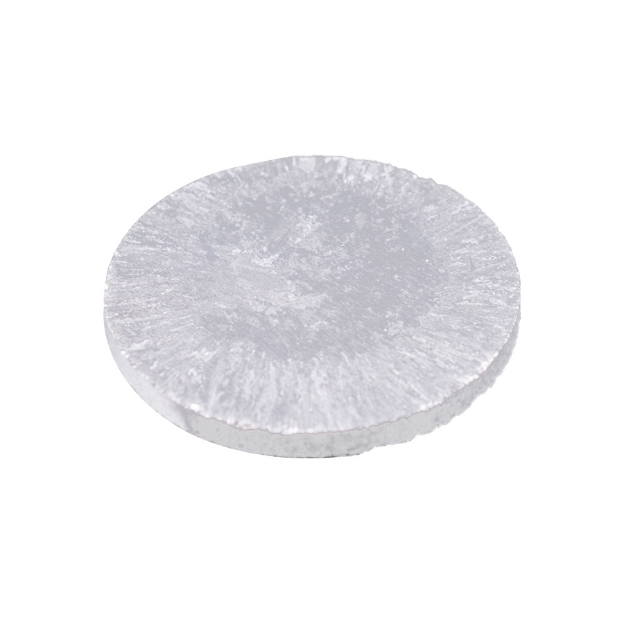
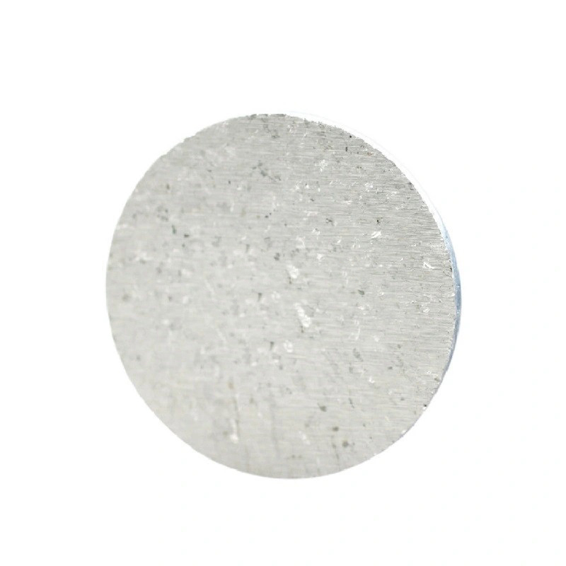
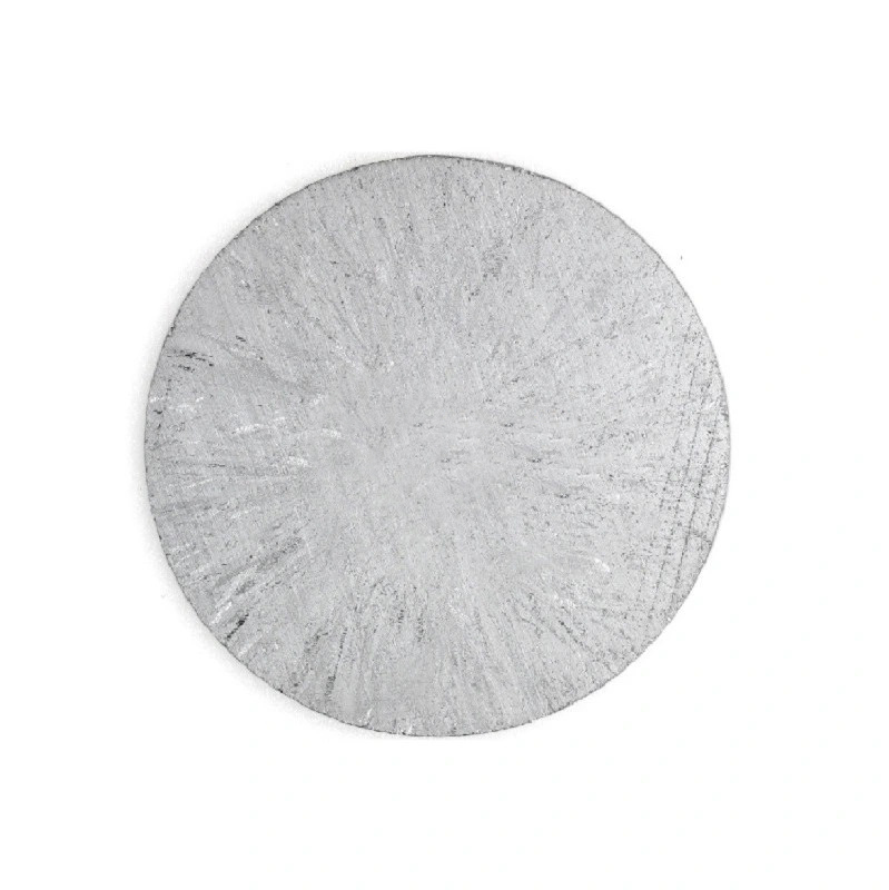
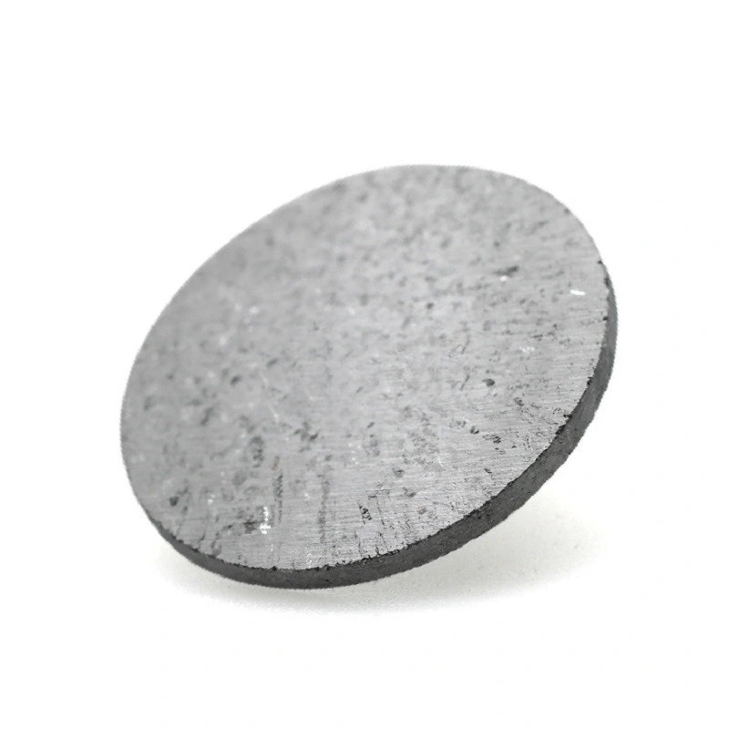
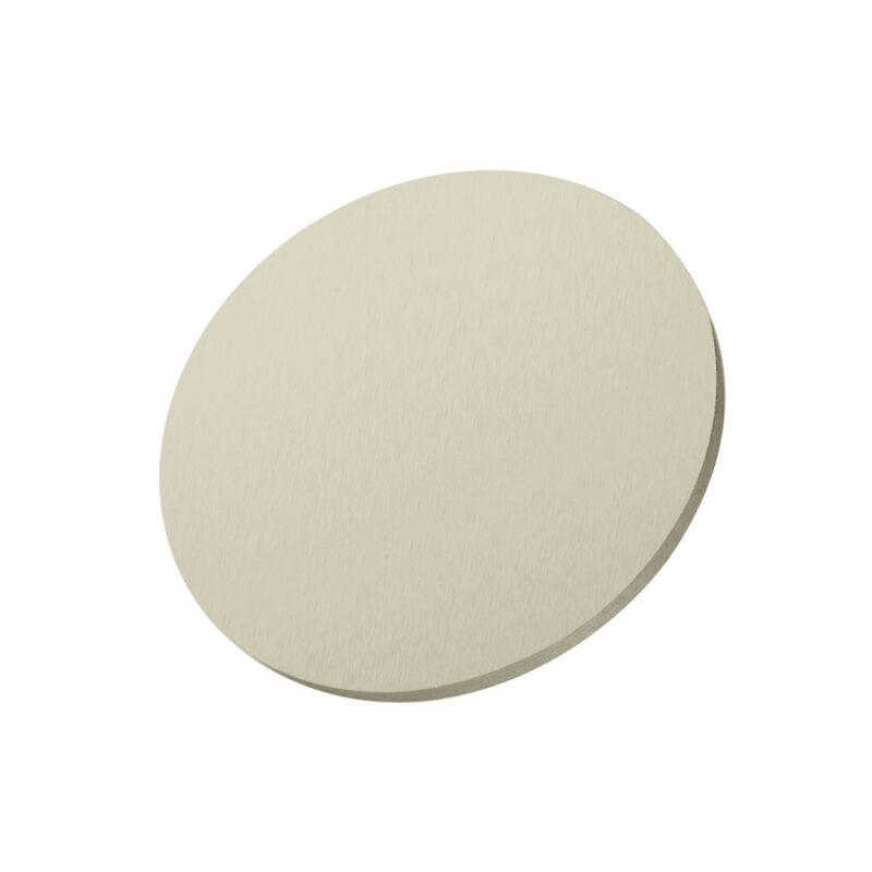
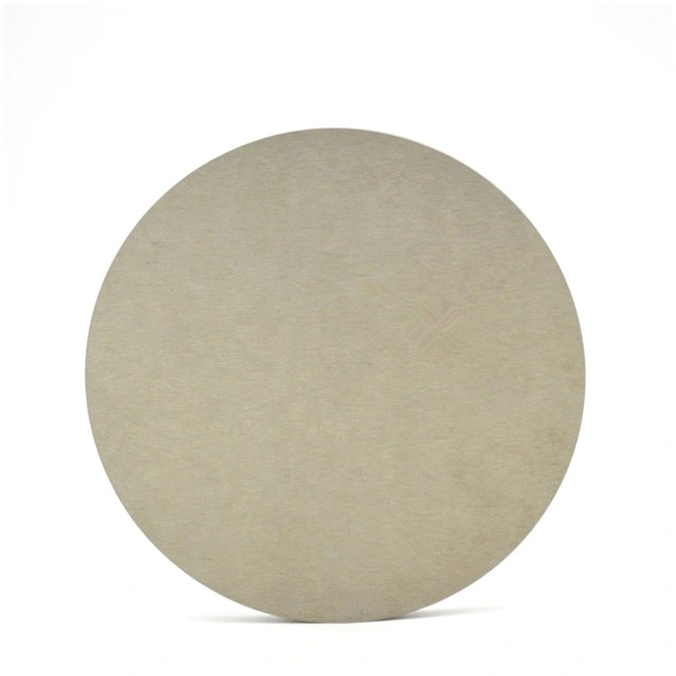
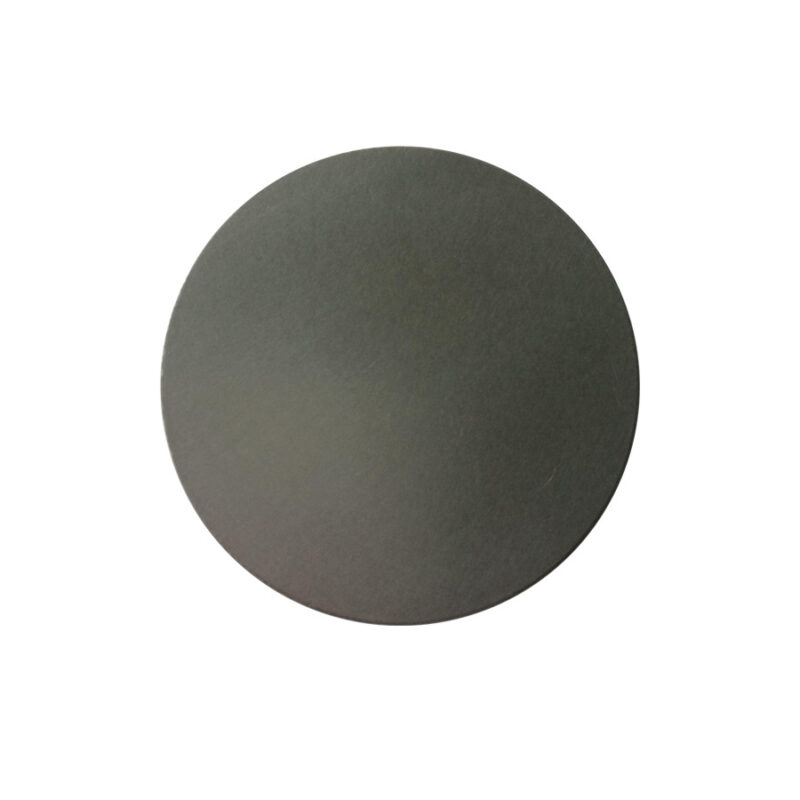
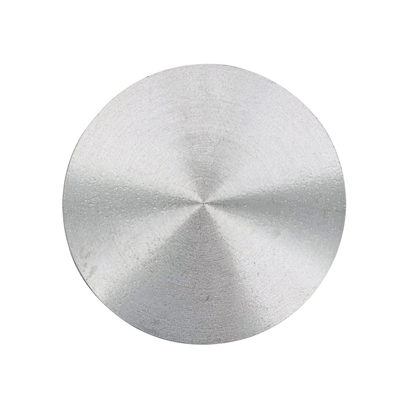
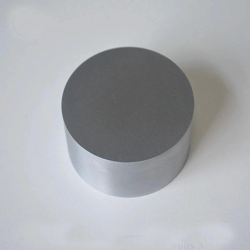
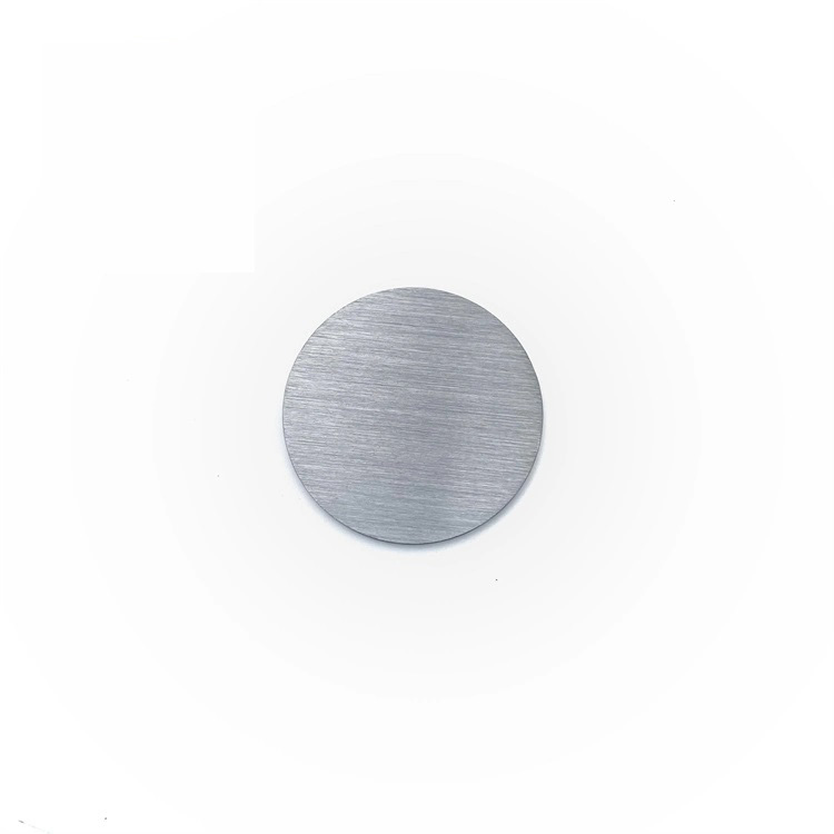
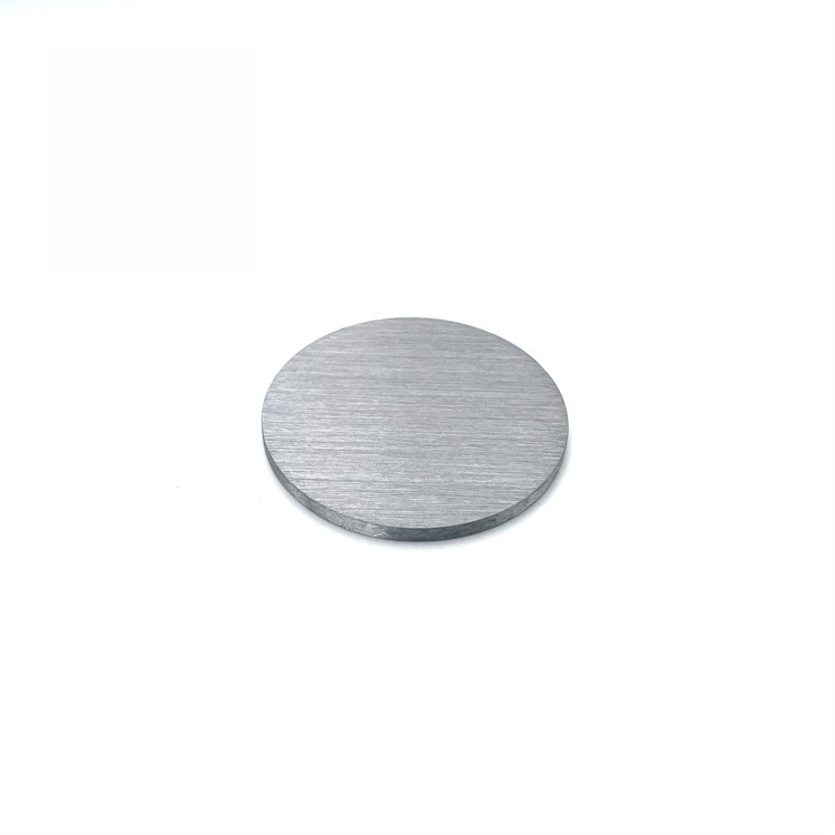
Sb Antimony Sputtering Target
- Thickness: The thickness of the stibium coating can be precisely controlled during the sputtering process, allowing for tailored solutions to meet specific application needs.
- Alloys: Stibium sputtering targets can be produced as pure antimony or in alloyed forms, such as antimony-tin (Sb-Sn) or antimony-lead (Sb-Pb), depending on the desired properties of the thin film.
- Backing Plates: Stibium targets can be bonded to backing plates made from materials like copper or molybdenum to improve thermal conductivity and mechanical stability during the sputtering process.
Custom products or bulk orders, please contact us for competitive pricing!
- Satisfaction Guaranteed
- No Hassle Refunds
- Secure Payments
Description
| Material | Antimony (Sb) |
| Purity | 99.99% – 99.9999% / 4N 4N5 5N 5N5 6N |
| Shape | disc, plate, sheet, rod, customized |
| Size | can be customized (contact us) |
| Package | vacuum bag or customer’s request |
| Place of Origin | China |
| MOQ | 1pcs |
| Supply Ability | 1000pcs per month |
| Lead Time | Qty: 1-100, Time: 3-10 days
Qty: >100, Time: to be negotiated |
Antimony ( Sb Stibium) sputtering targets are essential in industries that require materials with unique electrical, thermal, and optical properties, making them valuable in semiconductors, thermoelectric devices, batteries, and optical storage technologies.
Key Features:
- Purity: Antimony ( Sb Stibium) sputtering targets are typically available in high purity levels, such as 99.99% (4N) or higher, to ensure the deposition of high-quality and consistent films.
- Shapes and Sizes: These targets are available in various forms, including discs, plates, and custom shapes, to suit different sputtering systems and specific application requirements.
Applications:
- Semiconductor Devices: Stibium is used in the semiconductor industry for creating thin films in semiconductor devices, including diodes and infrared detectors, where it plays a role in modulating electrical properties and improving device performance.
- Thermoelectric Materials: Antimony is a key component in thermoelectric materials, where it is used to create thin films that can convert temperature differences into electrical energy. This makes it valuable in applications such as power generation and refrigeration.
- Alloy Formation: Stibium is commonly used to create alloys with other metals like tin (forming solder) or lead, enhancing properties such as strength and corrosion resistance. Sputtering these alloys allows for the precise control of film composition and thickness.
- Battery Technology: Antimony thin films are used in advanced battery technologies, particularly in solid-state batteries, where they help improve energy density and battery life.
- Optical Storage Devices: Antimony is used in the production of phase-change materials for optical storage devices, such as DVDs and Blu-ray discs, where its ability to rapidly change states under laser heating is essential for data recording.
Customization Options:
- Thickness: The thickness of the stibium coating can be precisely controlled during the sputtering process, allowing for tailored solutions to meet specific application needs.
- Alloys: Antimony ( Sb Stibium) sputtering targets can be produced as pure antimony or in alloyed forms, such as antimony-tin (Sb-Sn) or antimony-lead (Sb-Pb), depending on the desired properties of the thin film.
- Backing Plates: Antimony ( Sb Stibium) targets can be bonded to backing plates made from materials like copper or molybdenum to improve thermal conductivity and mechanical stability during the sputtering process.
Stibium sputtering targets, commonly known as antimony sputtering targets, are used in physical vapor deposition (PVD) processes to deposit thin antimony films onto various substrates. Antimony is a metalloid with unique properties, including good electrical conductivity and the ability to form alloys, making it valuable in a range of applications, particularly in the electronics and semiconductor industries.
If you have specific requirements, such as dimensions, purity, or application details, please contact us to match your needs.
