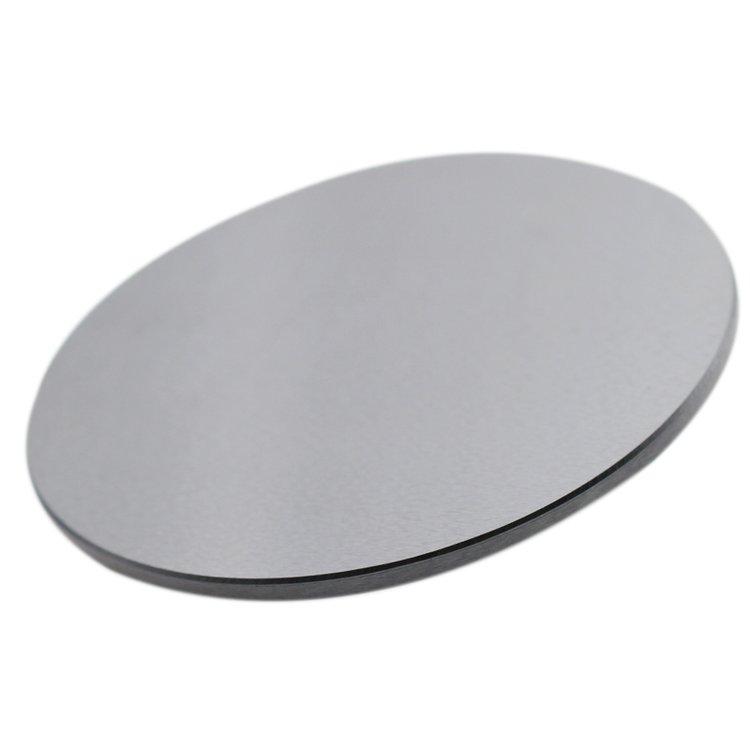
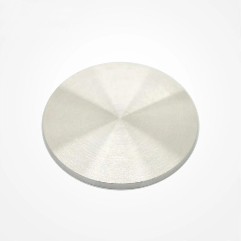
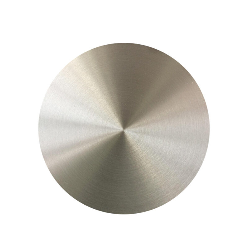
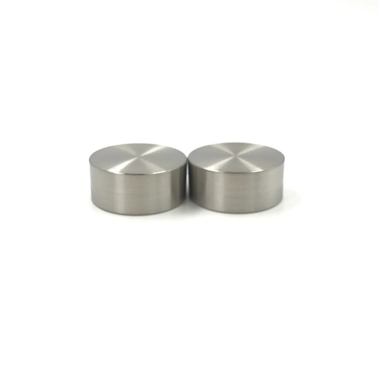
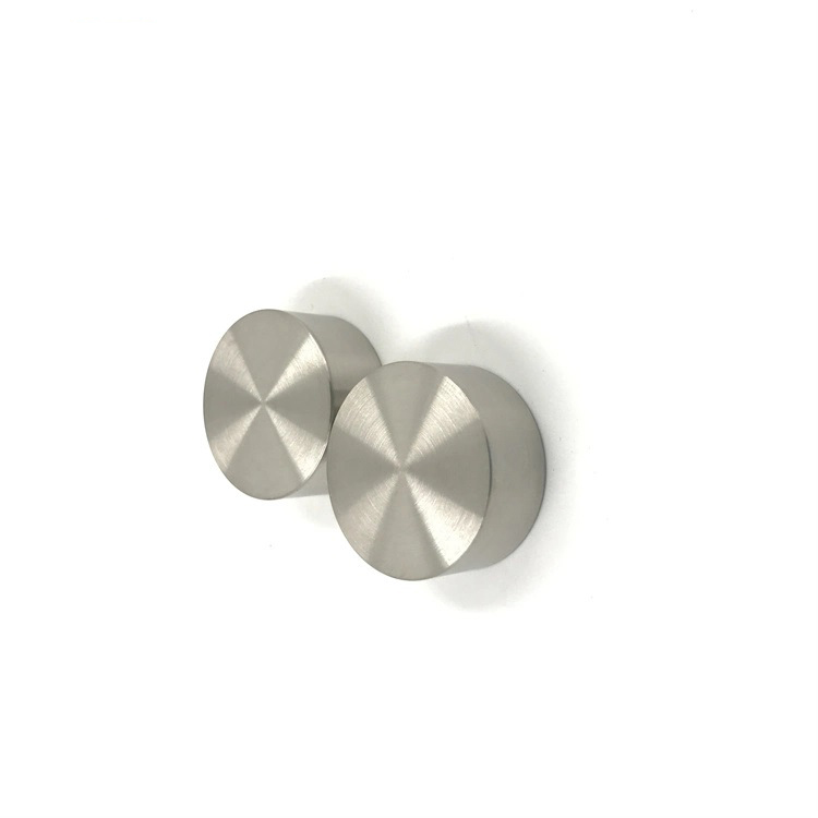
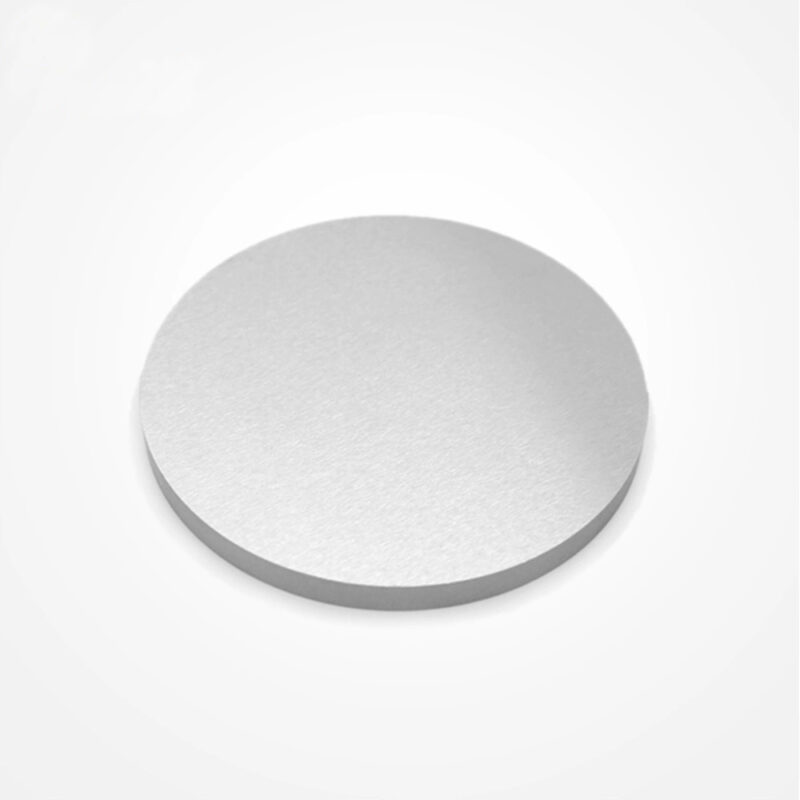
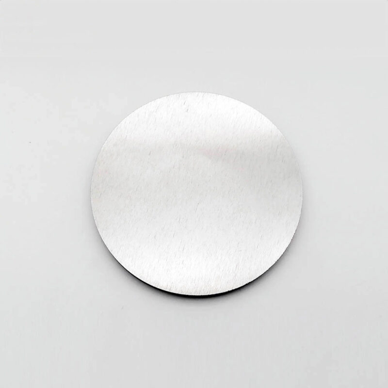
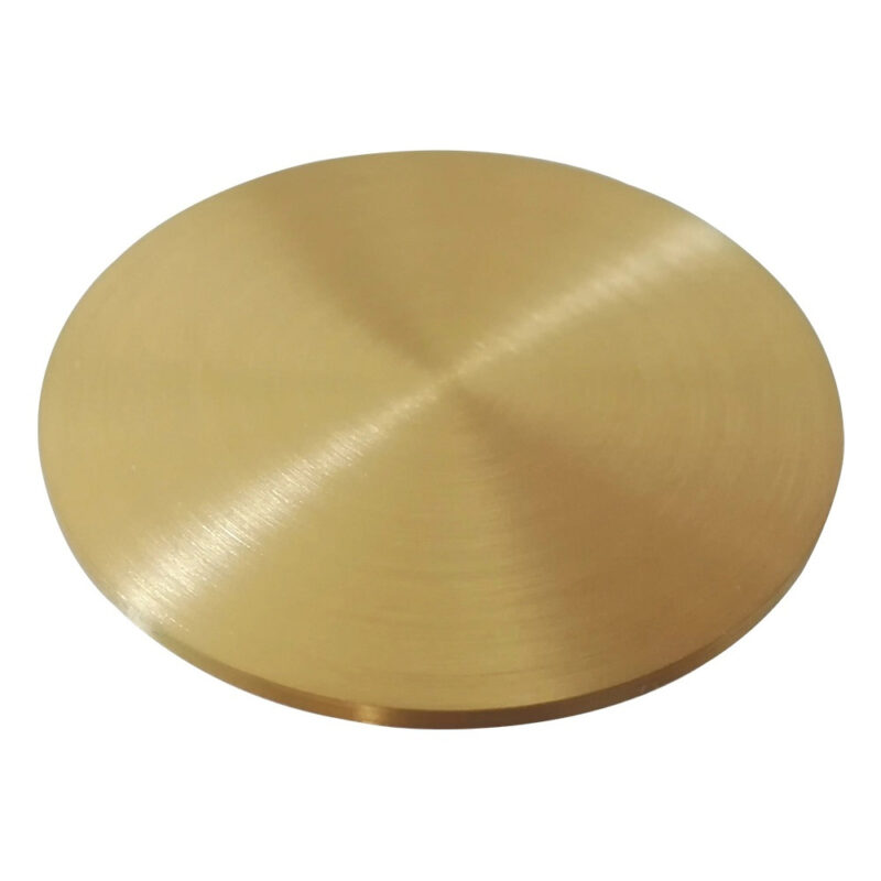
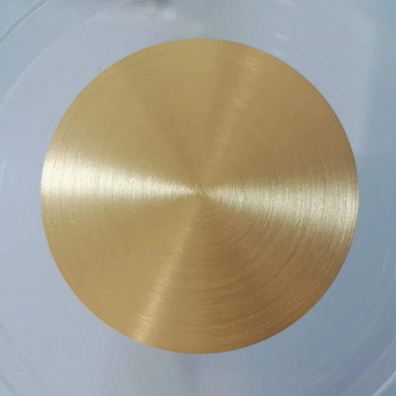
Bi2O2Se (Bismuth Oxyselenide) Sputtering Targets
- Layered Structure: Enables the exfoliation of thin films for various nanodevice applications.
- High Carrier Mobility: Supports rapid electron and hole movement for faster electronic response.
- Tunable Bandgap: Adjustable for different applications, optimizing its use in various electronic and optical devices.
- Good Thermal Stability: Suitable for high-temperature applications, enhancing long-term reliability.
Custom products or bulk orders, please contact us for competitive pricing!
- Satisfaction Guaranteed
- No Hassle Refunds
- Secure Payments
Description
| Material | Bismuth Oxyselenide (Bi₂O₂Se) |
| Purity | 99.5% – 99.9999% / 2N5 3N 3N5 4N 4N5 5N 5N5 6N |
| Shape | disc, plate, sheet, rod, customized |
| Size | can be customized (contact us) |
| Package | vacuum bag or customer’s request |
| MOQ | 1pcs |
| Supply Ability | 10000pcs per month |
| Lead Time | Qty: 1-100, Time: 3-10 days
Qty: >100, Time: to be negotiated |
Bismuth Oxyselenide (Bi₂O₂Se) is a unique semiconductor material with layered crystal structures. Known for its exceptional electronic, optical, and thermoelectric properties, it has gained significant attention in the fields of optoelectronics and nanoelectronics. As a sputtering target, Bi₂O₂Se is used in thin film deposition for various advanced technological applications.
Key Applications
- Thermoelectrics: Used in the development of efficient thermoelectric devices for energy conversion and cooling.
- Optoelectronics: Essential in photodetectors, light-emitting diodes (LEDs), and sensors.
- Nanoelectronics: Offers promising applications in the next generation of flexible and high-performance electronic devices.
- Research & Development: Utilized in fundamental studies of semiconductor properties and quantum phenomena.
Features and Benefits
- Layered Structure: Enables the exfoliation of thin films for various nanodevice applications.
- High Carrier Mobility: Supports rapid electron and hole movement for faster electronic response.
- Tunable Bandgap: Adjustable for different applications, optimizing its use in various electronic and optical devices.
- Good Thermal Stability: Suitable for high-temperature applications, enhancing long-term reliability.
Specifications
- Chemical Formula: Bi₂O₂Se
- Purity: ≥ 99.5%
- Crystal Structure: Tetragonal, layered
- Appearance: Typically gray or black powder/crystals
- Bandgap: Around 0.8 eV (can be adjusted)
- Density: Approx. 7.5 g/cm³
- Melting Point: 800°C (approx.)
Customization Options
- Purity Options: Custom purity levels available for specialized applications.
- Form: Available as powders, pellets, or custom sputtering targets to meet specific needs.
- Target Size: Custom dimensions to accommodate various sputtering systems.
- Research Assistance: Expert guidance on material usage and optimization for your specific application.
Unlock the potential of Bismuth Oxyselenide (Bi₂O₂Se) sputtering targets for your projects in optoelectronics, thermoelectrics, and advanced research. Contact us to learn more about how we can support your needs with high-quality materials and tailored solutions.
