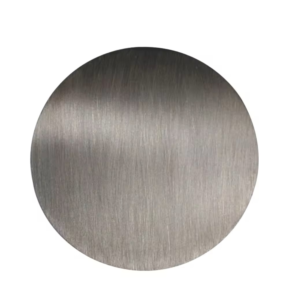
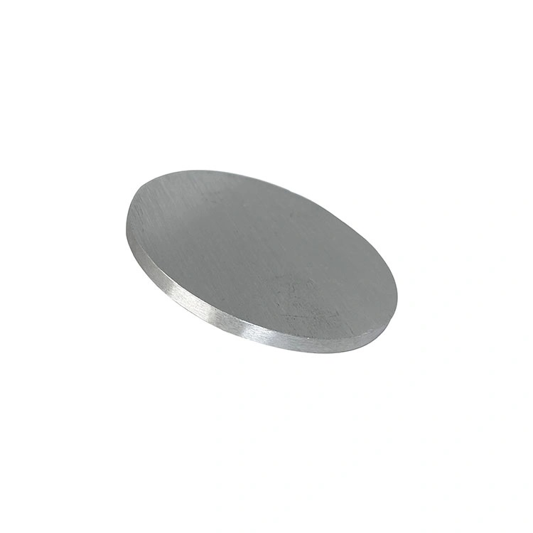
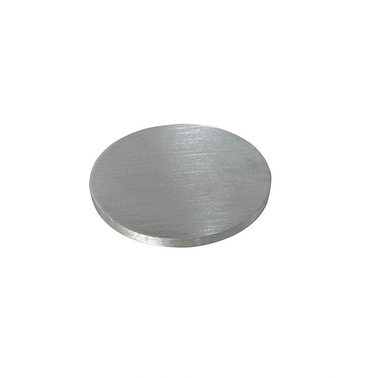
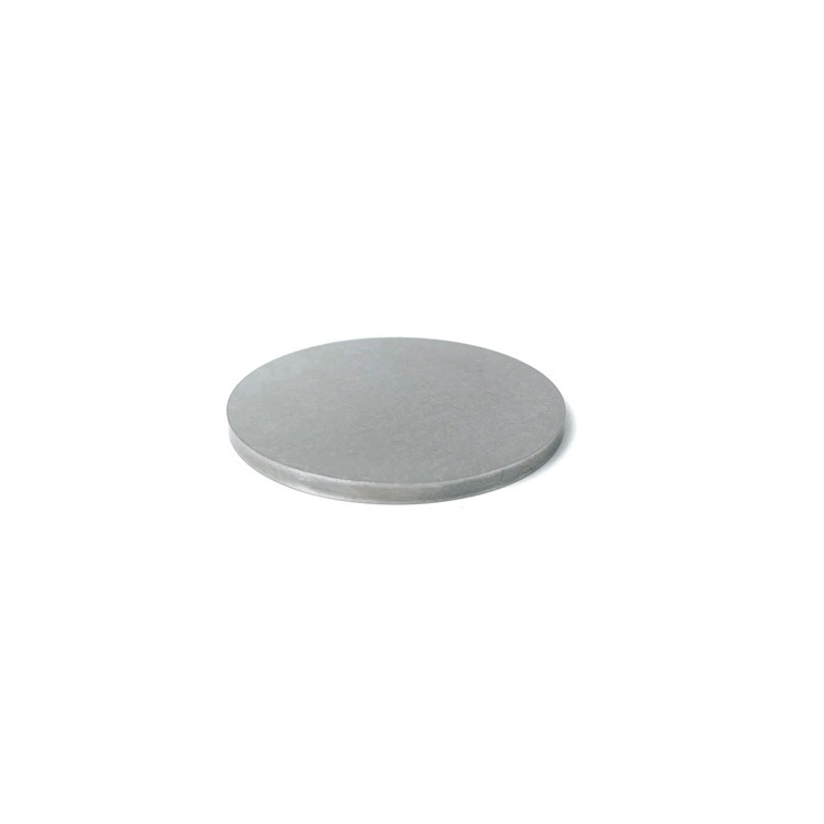
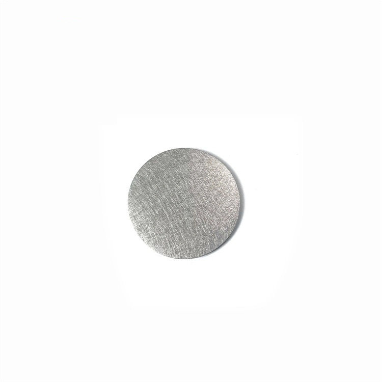
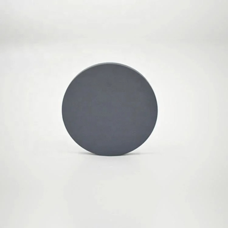
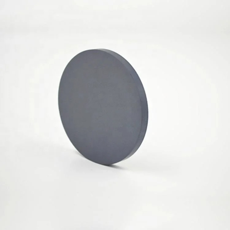
Bi2Se3 (Bismuth Selenide) Sputtering Target
- Topological Insulator Properties: Bi₂Se₃ is known for its topological insulator characteristics, where it supports surface conduction while acting as an insulator in its bulk, opening pathways for advanced quantum applications.
- Thermoelectric Efficiency: Bi₂Se₃ exhibits excellent thermoelectric performance with a high Seebeck coefficient, making it a critical material for thermoelectric energy conversion.
- Low Thermal Conductivity: Its low thermal conductivity helps in maximizing the thermoelectric efficiency in power generation and cooling applications.
- High IR Sensitivity: Bi₂Se₃’s sensitivity to infrared radiation makes it ideal for IR sensors and other optoelectronic devices.
Custom products or bulk orders, please contact us for competitive pricing!
- Satisfaction Guaranteed
- No Hassle Refunds
- Secure Payments
Description
| Material | Bi2Se3 |
| Purity | 99.9% – 99.9999% / 3N 3N5 4N 4N5 5N 5N5 6N |
| Shape | disc, plate, sheet, rod, customized |
| Size | can be customized (contact us) |
| Package | vacuum bag or customer’s request |
| Place of Origin | China |
| MOQ | 1pcs |
| Supply Ability | 10000pcs per month |
| Lead Time | Qty: 1-100, Time: 3-10 days
Qty: >100, Time: to be negotiated |
Bi₂Se₃ (Bismuth Selenide) sputtering targets are primarily used in the production of thin films for advanced electronic, thermoelectric, and optoelectronic applications. Bismuth selenide is a well-known topological insulator material that exhibits unique properties such as surface states protected by time-reversal symmetry, making it valuable in quantum computing and spintronic devices.
Key Applications:
- Thermoelectric Devices: Bi₂Se₃ is used to create thermoelectric films that convert temperature differences into electrical voltage, making it essential for power generation and cooling technologies.
- Topological Insulators: Bi₂Se₃ is a prominent material in the study of topological insulators, which have potential applications in quantum computing due to their ability to conduct electrical current on their surface while remaining insulating in the bulk.
- Spintronic Devices: The spin-dependent electrical properties of Bi₂Se₃ make it useful in the development of spintronics, where the spin of electrons is used for data storage and transmission, potentially leading to faster and more efficient electronic devices.
- Infrared Detectors: Due to its narrow bandgap and good thermoelectric properties, Bi₂Se₃ is also employed in infrared (IR) detectors and sensors for industrial and military applications.
Features of Bi₂Se₃ Sputtering Targets:
- Topological Insulator Properties: Bi₂Se₃ is known for its topological insulator characteristics, where it supports surface conduction while acting as an insulator in its bulk, opening pathways for advanced quantum applications.
- Thermoelectric Efficiency: Bi₂Se₃ exhibits excellent thermoelectric performance with a high Seebeck coefficient, making it a critical material for thermoelectric energy conversion.
- Low Thermal Conductivity: Its low thermal conductivity helps in maximizing the thermoelectric efficiency in power generation and cooling applications.
- High IR Sensitivity: Bi₂Se₃’s sensitivity to infrared radiation makes it ideal for IR sensors and other optoelectronic devices.
Customization Options:
- Target Sizes: Bi₂Se₃ sputtering targets can be customized to fit various sputtering systems and deposition needs, available in different shapes and dimensions.
- High Purity: High-purity Bi₂Se₃ targets ensure consistent, high-performance thin films, critical for research and industrial applications in quantum devices and thermoelectrics.
- Bonding Services: Bonding to a backing plate is available to improve thermal management and prevent cracking during sputtering processes.
Bi₂Se₃ (Bismuth Selenide) sputtering targets from Tinsan Materials are ideal for thermoelectric, topological insulator, and optoelectronic applications. Offering high thermoelectric efficiency and advanced surface conduction properties, these targets are used in quantum computing, spintronics, and IR sensors. Available in custom sizes and high-purity options.
If you have specific requirements, such as dimensions, purity, or application details, please contact us to match your needs.
