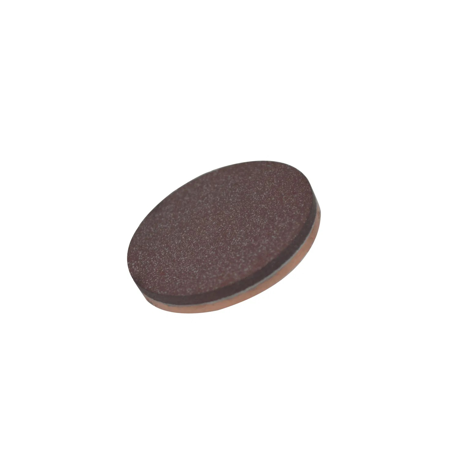
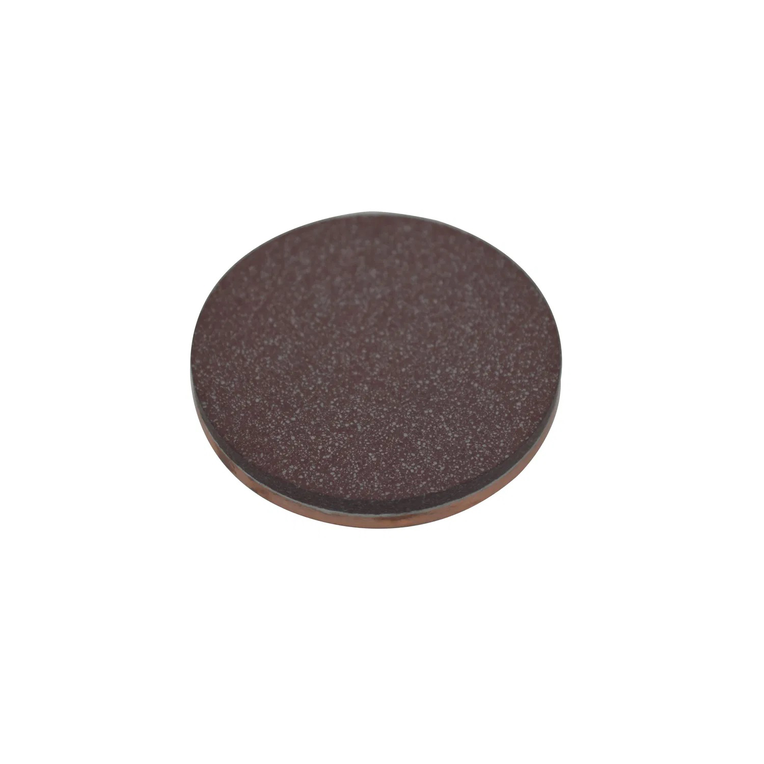
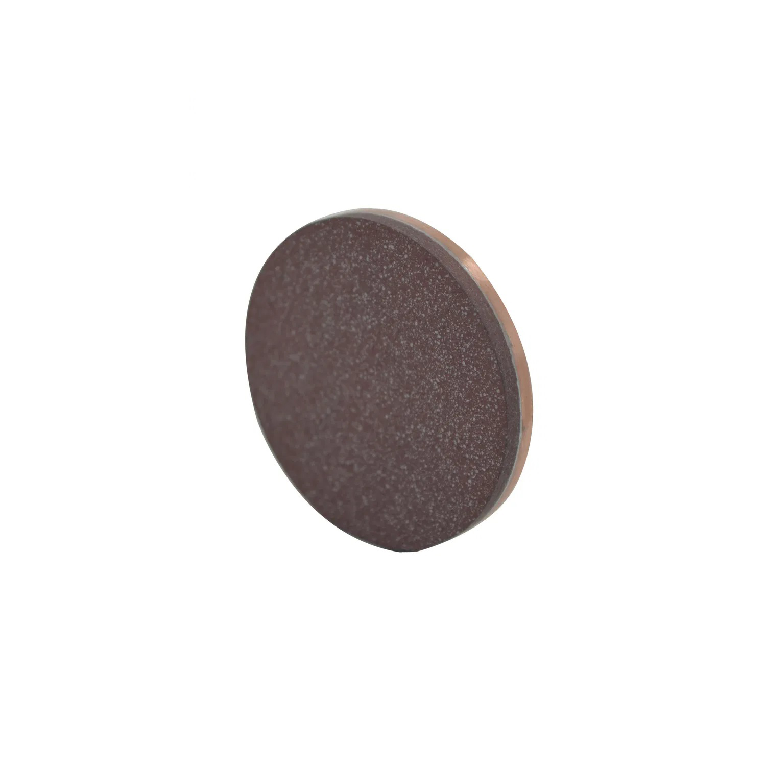
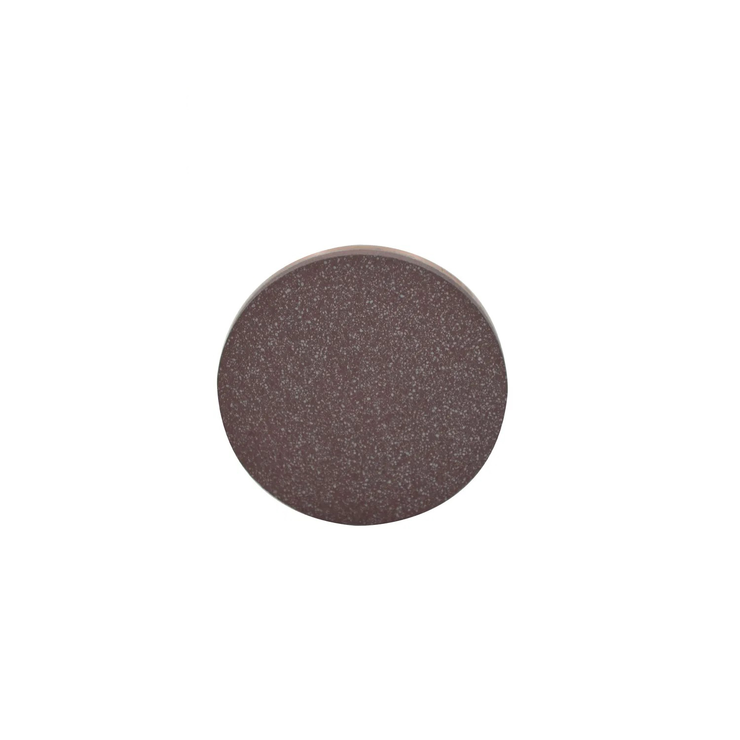
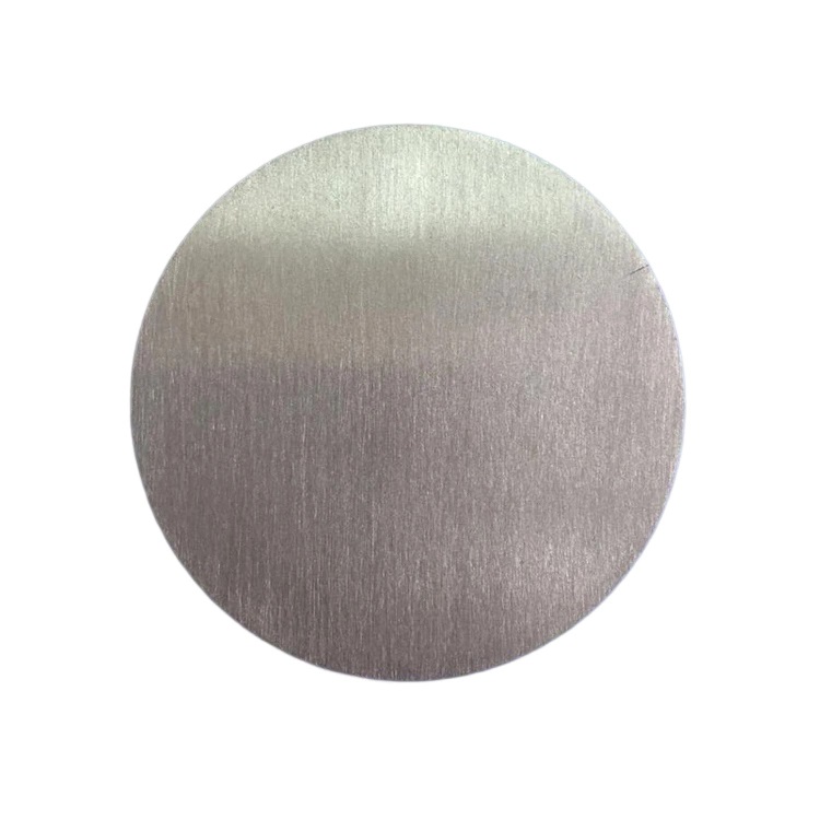
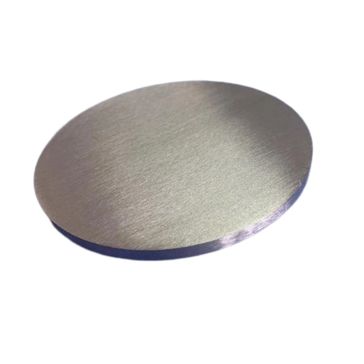
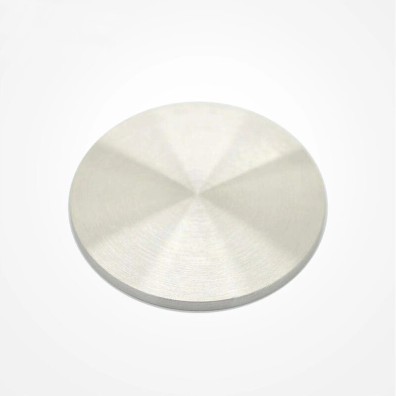
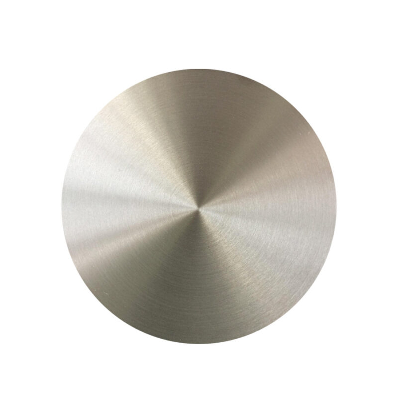
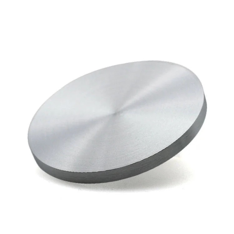
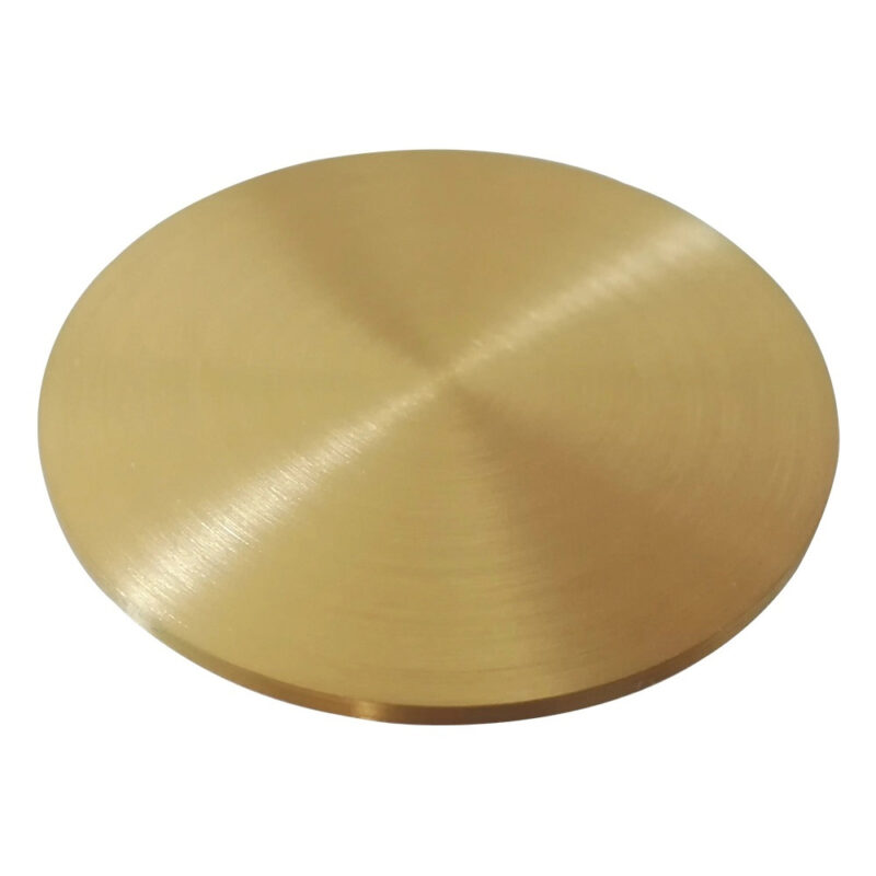
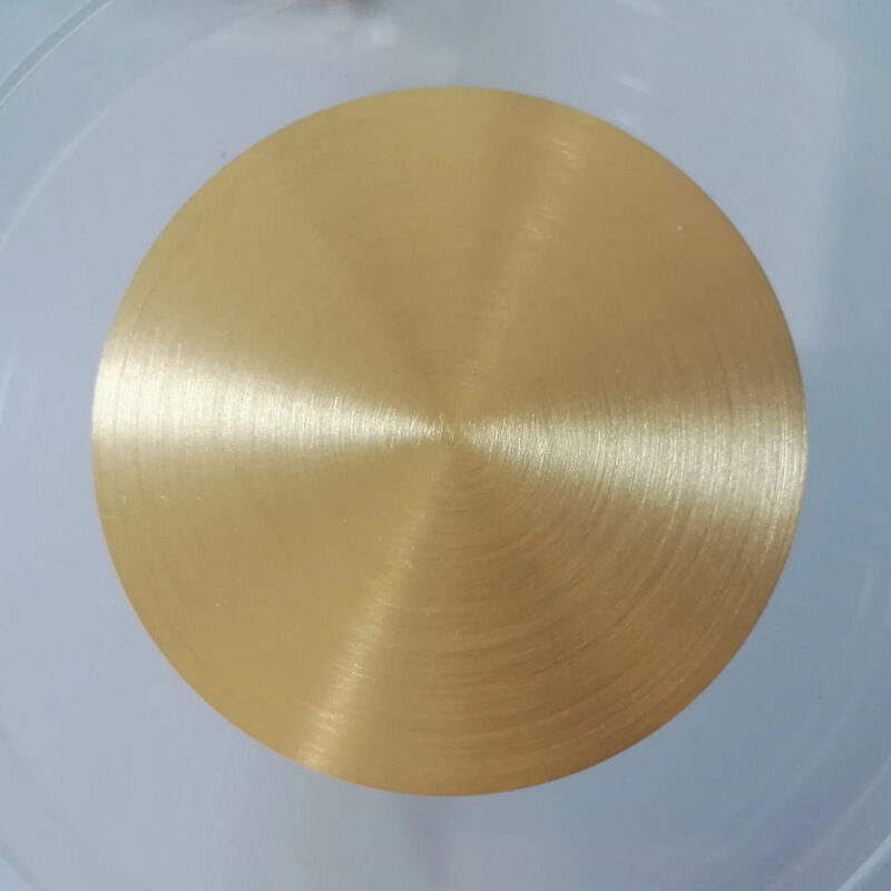
BiFeO3 (Bismuth Ferrite) Sputtering Target
- Multiferroic Properties: BiFeO₃ demonstrates both ferroelectric and antiferromagnetic properties, making it ideal for multifunctional devices.
- Room Temperature Functionality: One of the few multiferroic materials that operates effectively at room temperature, allowing for broader application in consumer electronics and industrial devices.
- Photovoltaic Effects: BiFeO₃ can be used to create thin films that convert light into electricity, opening avenues for energy harvesting and improving photovoltaic technologies.
- Customizable: The size, shape, and purity of BiFeO₃ sputtering targets can be tailored to meet specific requirements for various deposition techniques.
Custom products or bulk orders, please contact us for competitive pricing!
- Satisfaction Guaranteed
- No Hassle Refunds
- Secure Payments
Description
| Material | BiFeO3 |
| Purity | 99.9% – 99.9999% / 3N 3N5 4N 4N5 5N 5N5 6N |
| Shape | disc, plate, sheet, rod, customized |
| Size | can be customized (contact us) |
| Package | vacuum bag or customer’s request |
| Place of Origin | China |
| MOQ | 1pcs |
| Supply Ability | 10000pcs per month |
| Lead Time | Qty: 1-100, Time: 3-10 days
Qty: >100, Time: to be negotiated |
Bismuth Ferrite (BiFeO₃ or BFO) sputtering targets are widely used in thin-film deposition for applications in multiferroic materials, sensors, optoelectronic devices, and spintronics. BiFeO₃ is a unique material known for exhibiting both ferroelectric and antiferromagnetic properties, making it highly suitable for advanced electronics and memory devices.
Key Applications:
- Multiferroic Devices: BiFeO₃ is one of the few materials that exhibit both ferroelectricity and antiferromagnetism at room temperature, making it ideal for use in multiferroic memory devices, which can store data magnetically and electrically.
- Sensors: Due to its multiferroic nature, BiFeO₃ is utilized in various types of sensors, especially those requiring a combination of electrical and magnetic responsiveness.
- Spintronics: In spintronic devices, BiFeO₃ is used to control electron spin states, contributing to the development of next-generation computing devices that are faster and more energy-efficient.
- Photovoltaics: BiFeO₃ thin films can be used in solar energy conversion due to their ability to generate photovoltaic effects, improving the performance of solar cells and other energy-harvesting devices.
- Optoelectronic Devices: BiFeO₃ is also valuable in optoelectronics, where it is used to modulate light in devices such as modulators, sensors, and photodetectors.
Features of BiFeO₃ Sputtering Targets:
- Multiferroic Properties: BiFeO₃ demonstrates both ferroelectric and antiferromagnetic properties, making it ideal for multifunctional devices.
- Room Temperature Functionality: One of the few multiferroic materials that operates effectively at room temperature, allowing for broader application in consumer electronics and industrial devices.
- Photovoltaic Effects: BiFeO₃ can be used to create thin films that convert light into electricity, opening avenues for energy harvesting and improving photovoltaic technologies.
- Customizable: The size, shape, and purity of BiFeO₃ sputtering targets can be tailored to meet specific requirements for various deposition techniques.
Customization Options:
- Target Sizes: Available in a variety of shapes, such as circular, rectangular, or custom sizes, to fit different sputtering systems.
- Purity Levels: BiFeO₃ sputtering targets can be produced with high purity, ensuring high-quality films for advanced technological applications.
- Bonding Options: BiFeO₃ targets can be bonded to backing plates for better thermal management during the sputtering process, reducing the risk of cracking or other damage.
BiFeO₃ (Bismuth Ferrite) sputtering targets from Tinsan Materials offer high-quality thin films for multiferroic devices, sensors, spintronics, and optoelectronics. With ferroelectric and antiferromagnetic properties, room temperature functionality, and customizable target sizes, BiFeO₃ targets are ideal for advanced electronics, memory devices, and photovoltaic applications.
If you have specific requirements, such as dimensions, purity, or application details, please contact us to match your needs.
