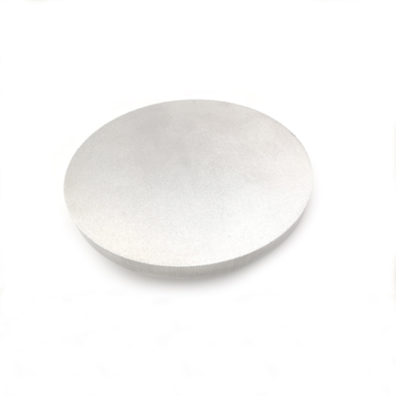
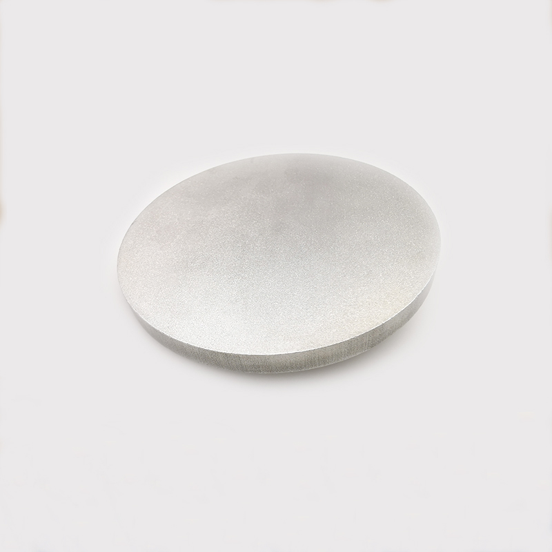
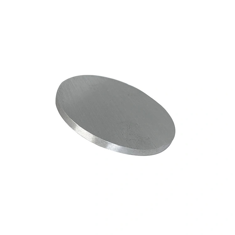
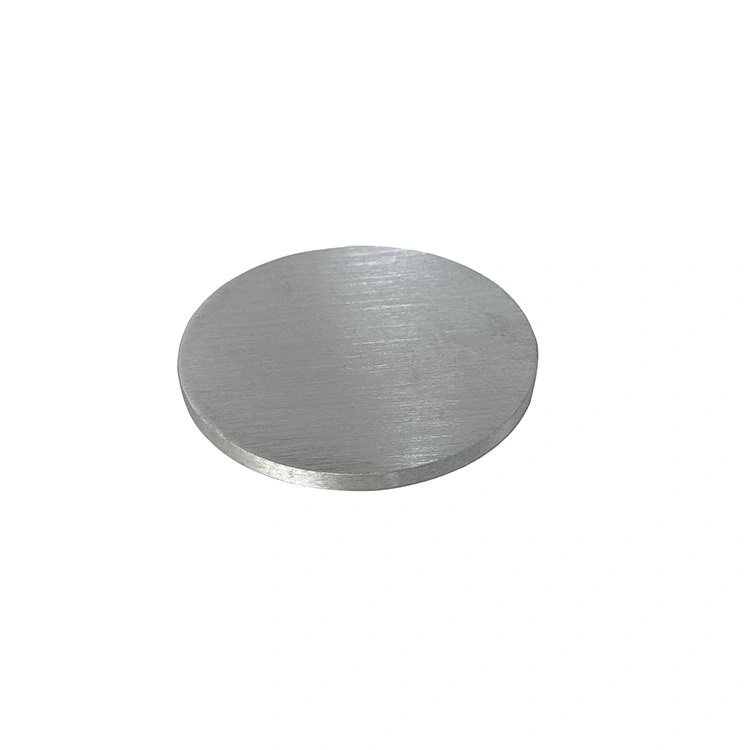
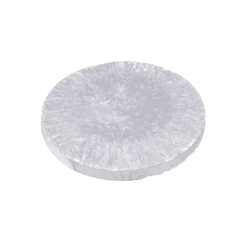
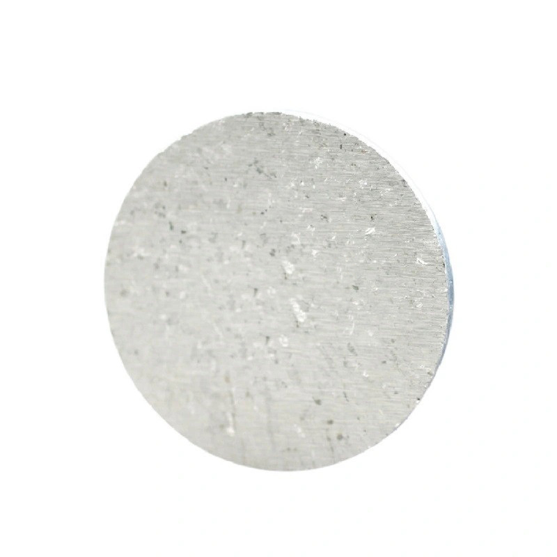
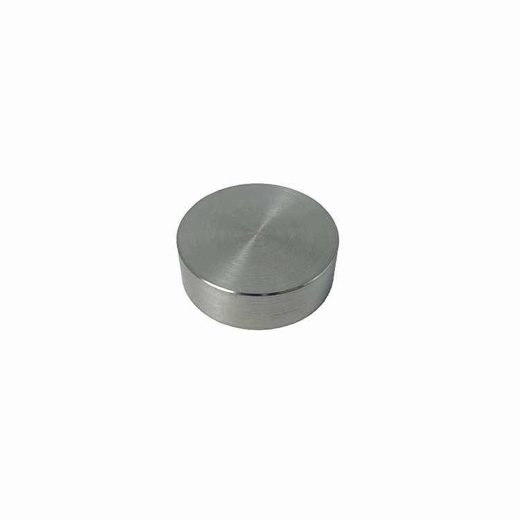
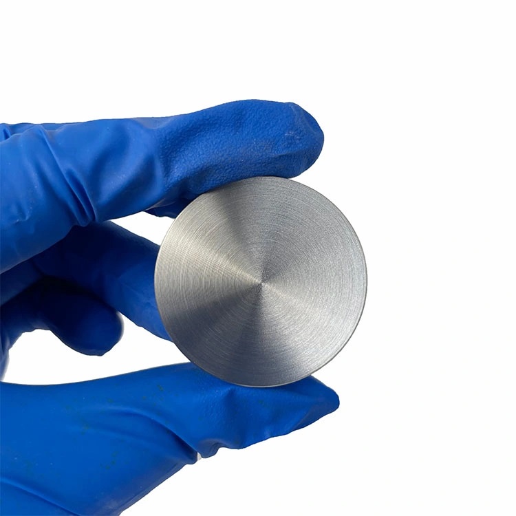
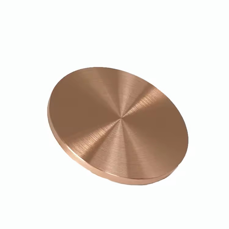
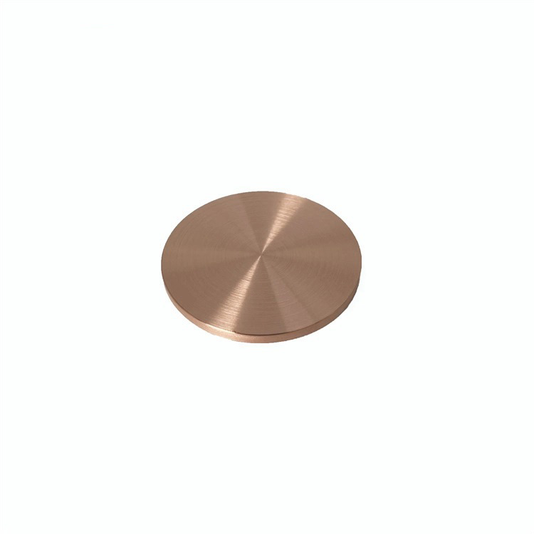
Cd Cadmium Metal Sputtering Targets
- Shapes Available: Circular (disc), rectangular, and custom-designed targets.
- Diameter Range: Custom sizes available.
- Thickness: Varies depending on application requirements.
- Surface Finish: Fine-polished to ensure uniform film deposition.
- Backing Plate: Available with or without bonding to enhance thermal and mechanical stability.
Custom products or bulk orders, please contact us for competitive pricing!
- Satisfaction Guaranteed
- No Hassle Refunds
- Secure Payments
Description
| Material | Cadmium (Cd) |
| Purity | 99.9% – 99.999% / 3N 3N5 4N 4N5 5N |
| Shape | disc, plate, sheet, rod, customized |
| Size | can be customized (contact us) |
| Package | vacuum bag or customer’s request |
| MOQ | 1pcs |
| Lead Time | Qty: 1-100, Time: 3-10 days
Qty: >100, Time: to be negotiated |
Cadmium (Cd) Sputtering Targets are high-purity materials used in thin-film deposition processes, including Physical Vapor Deposition (PVD) methods such as sputtering and thermal evaporation. These targets are widely applied in the semiconductor industry, optical coatings, photovoltaic cells, and electronic components. Our Cd sputtering targets are available in various shapes and sizes, with a purity of up to 99.999% (5N), ensuring excellent film quality and performance.
Material Properties
- Chemical Symbol: Cd
- Atomic Number: 48
- Density: 8.65 g/cm³
- Melting Point: 321.1°C
- Boiling Point: 767°C
- Purity Levels: 99.9% (3N), 99.99% (4N), 99.999% (5N)
- Electrical Conductivity: High conductivity for electronic applications
- Corrosion Resistance: Resistant to oxidation under controlled environments
Applications
Cadmium sputtering targets are utilized in various industries due to their unique properties:
- Photovoltaics: Essential in CdTe (Cadmium Telluride) thin-film solar cells, known for their high efficiency and cost-effectiveness.
- Optical Coatings: Used in anti-reflective and protective coatings for lenses, mirrors, and optical instruments.
- Semiconductor Industry: Applied in compound semiconductors and advanced electronic devices.
- Thin-Film Deposition: Utilized in research and development for new material coatings in nanotechnology and high-tech applications.
Product Specifications
- Shapes Available: Circular (disc), rectangular, and custom-designed targets.
- Diameter Range: Custom sizes available.
- Thickness: Varies depending on application requirements.
- Surface Finish: Fine-polished to ensure uniform film deposition.
- Backing Plate: Available with or without bonding to enhance thermal and mechanical stability.
Quality Control & Testing
To ensure the highest quality, our cadmium sputtering targets undergo rigorous testing, including:
- Chemical Purity Analysis: Verified using X-ray fluorescence spectroscopy (XRF) and Inductively Coupled Plasma Mass Spectrometry (ICP-MS).
- Dimensional Accuracy: Precision machining to meet exact customer specifications.
- Surface Quality Inspection: Ensuring low roughness (Ra) for optimal thin-film uniformity.
Packaging & Storage
- Individually vacuum-sealed to prevent contamination and oxidation.
- Packed in anti-static, moisture-proof materials for secure transportation.
- Recommended storage in a cool, dry environment to maintain integrity.
Ordering & Delivery
- Customization: Available for specific shapes, sizes, and purity levels.
- Minimum Order Quantity (MOQ): Flexible based on customer needs.
- Lead Time: Typically 1-2 weeks, depending on specifications.
- Shipping: Worldwide delivery with secure packaging and handling.
If you have specific requirements, such as dimensions, purity, or application details, please contact us to match your needs.
