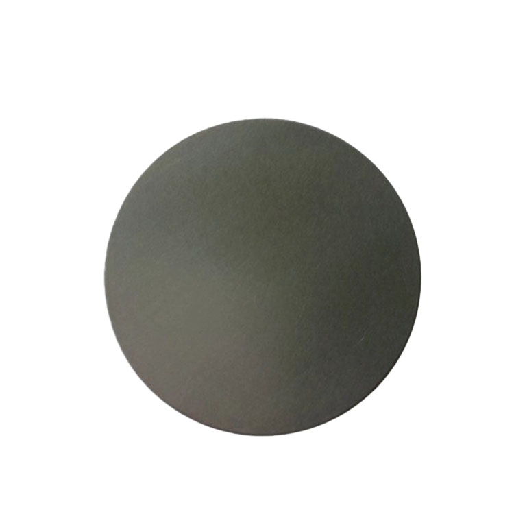
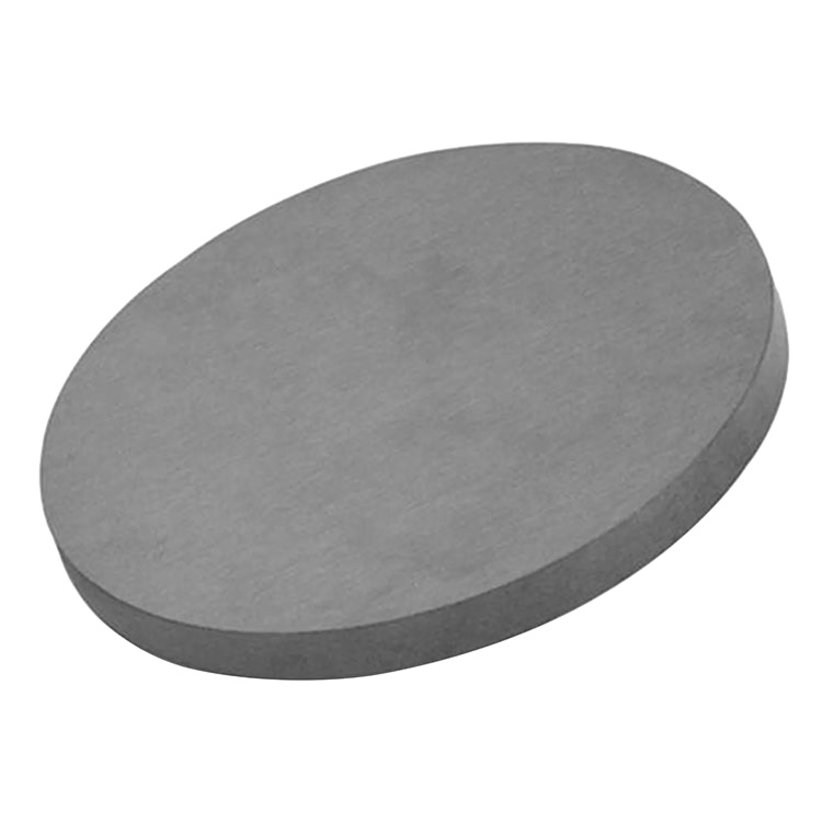
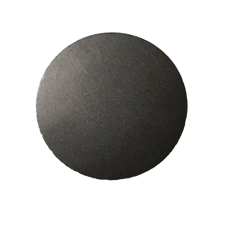
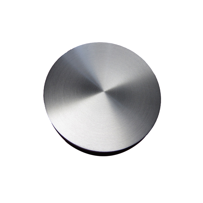
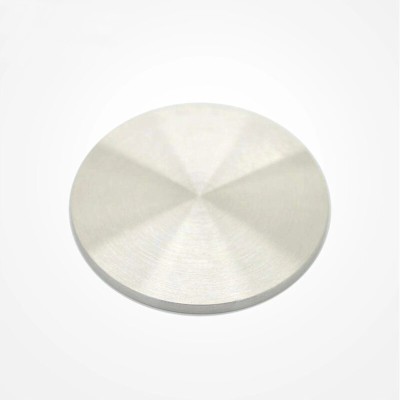
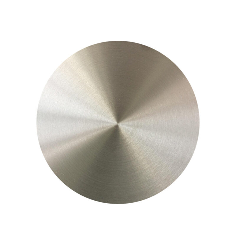
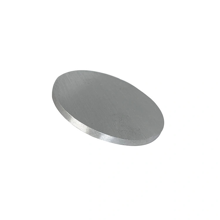
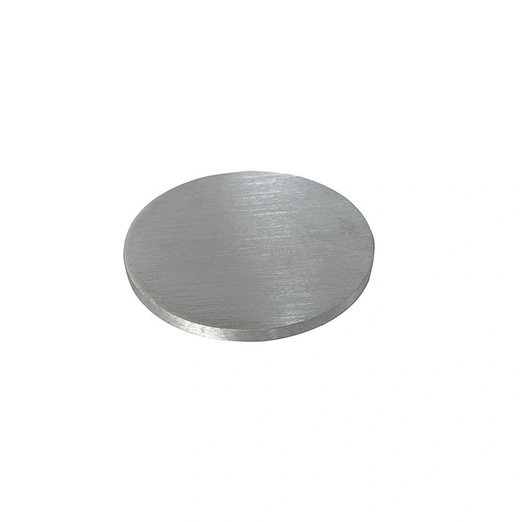
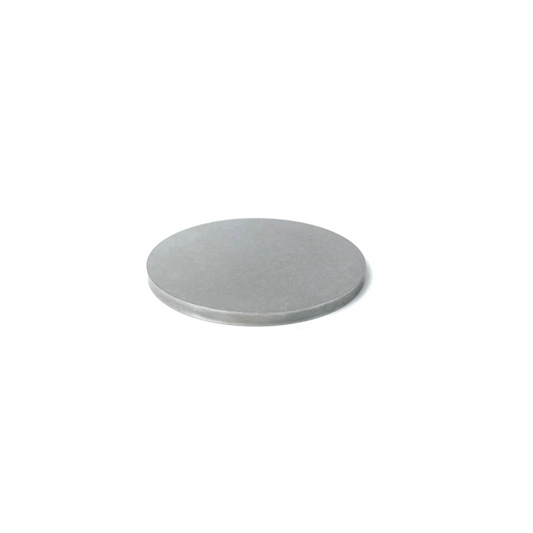
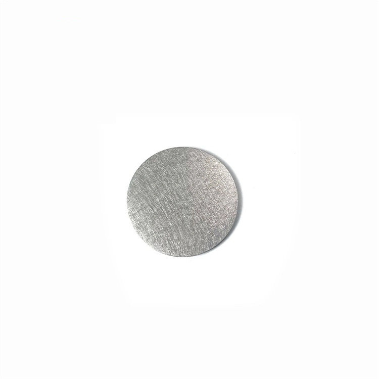
CdS (Cadmium Sulfide) Sputtering Target
- Direct Bandgap Semiconductor: CdS has a direct bandgap (~2.42 eV), making it an excellent material for optoelectronic applications requiring high-efficiency light absorption and emission.
- High Transparency: CdS exhibits high transparency in the visible spectrum, making it an ideal candidate for window layers in photovoltaic devices.
- Stable and Efficient: CdS is a stable semiconductor with efficient electron-hole pair generation, which enhances the performance of solar cells and optoelectronic devices.
- Low-cost Semiconductor: Compared to other semiconductors, CdS offers a cost-effective solution for large-scale production in photovoltaics and other electronics.
Custom products or bulk orders, please contact us for competitive pricing!
- Satisfaction Guaranteed
- No Hassle Refunds
- Secure Payments
Description
| Material | Cadmium Sulfide |
| Purity | 99.9% – 99.9999% / 3N 3N5 4N 4N5 5N 5N5 6N |
| Shape | disc, plate, sheet, rod, customized |
| Size | can be customized (contact us) |
| Package | vacuum bag or customer’s request |
| Place of Origin | China |
| MOQ | 1pcs |
| Supply Ability | 10000pcs per month |
| Lead Time | Qty: 1-100, Time: 3-10 days
Qty: >100, Time: to be negotiated |
CdS (Cadmium Sulfide) sputtering targets are widely used for thin-film deposition in optoelectronics, solar cells, and semiconductors. Cadmium Sulfide is a II-VI semiconductor with a direct bandgap, making it an essential material for devices that require efficient light absorption and emission.
Key Applications:
- Photovoltaics: CdS is commonly used as a window layer material in thin-film solar cells, particularly in CdTe and CIGS (Copper Indium Gallium Selenide) solar cells. Its optical properties make it ideal for improving the efficiency of solar energy conversion.
- Optoelectronics: CdS is used in light-emitting diodes (LEDs), lasers, and photodetectors, due to its ability to efficiently absorb and emit light. It is also used in quantum dot devices.
- Thin-film Transistors: CdS thin films are employed in the fabrication of thin-film transistors (TFTs), which are crucial for displays, including flexible electronics.
- Photocatalysis: CdS is used in photocatalytic applications, especially for water splitting and environmental remediation, due to its semiconductor properties and effective absorption in the visible light range.
- Quantum Dots: CdS is a core material in the production of quantum dots, offering tunable emission properties depending on the size of the quantum dots, making it highly applicable in advanced display technologies and medical imaging.
Features of CdS Sputtering Targets:
- Direct Bandgap Semiconductor: CdS has a direct bandgap (~2.42 eV), making it an excellent material for optoelectronic applications requiring high-efficiency light absorption and emission.
- High Transparency: CdS exhibits high transparency in the visible spectrum, making it an ideal candidate for window layers in photovoltaic devices.
- Stable and Efficient: CdS is a stable semiconductor with efficient electron-hole pair generation, which enhances the performance of solar cells and optoelectronic devices.
- Low-cost Semiconductor: Compared to other semiconductors, CdS offers a cost-effective solution for large-scale production in photovoltaics and other electronics.
Customization Options:
- Dimensions: CdS sputtering targets can be customized in different shapes and sizes, such as discs, plates, and custom geometries, to meet specific sputtering requirements.
- Purity: High-purity CdS targets (up to 99.999%) are available for applications requiring minimal impurities for optimal device performance.
- Doping: CdS can be doped with other elements to modify its electronic and optical properties, enhancing its suitability for various applications like thin-film transistors and optoelectronics.
CdS (Cadmium Sulfide) sputtering targets from Tinsan Materials offer high purity and customizable sizes for use in photovoltaics, quantum dots, optoelectronics, and thin-film transistors. Ideal for solar cells and advanced optoelectronic devices.
If you have specific requirements, such as dimensions, purity, or application details, please contact us to match your needs.
