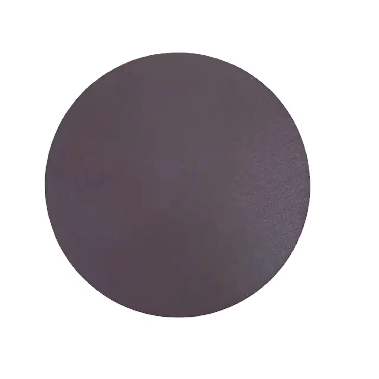
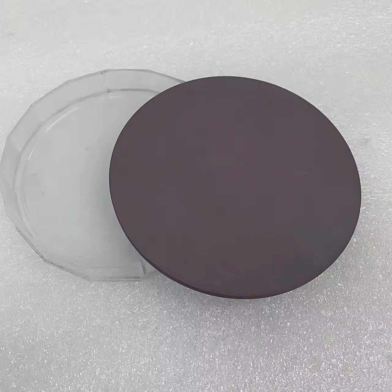
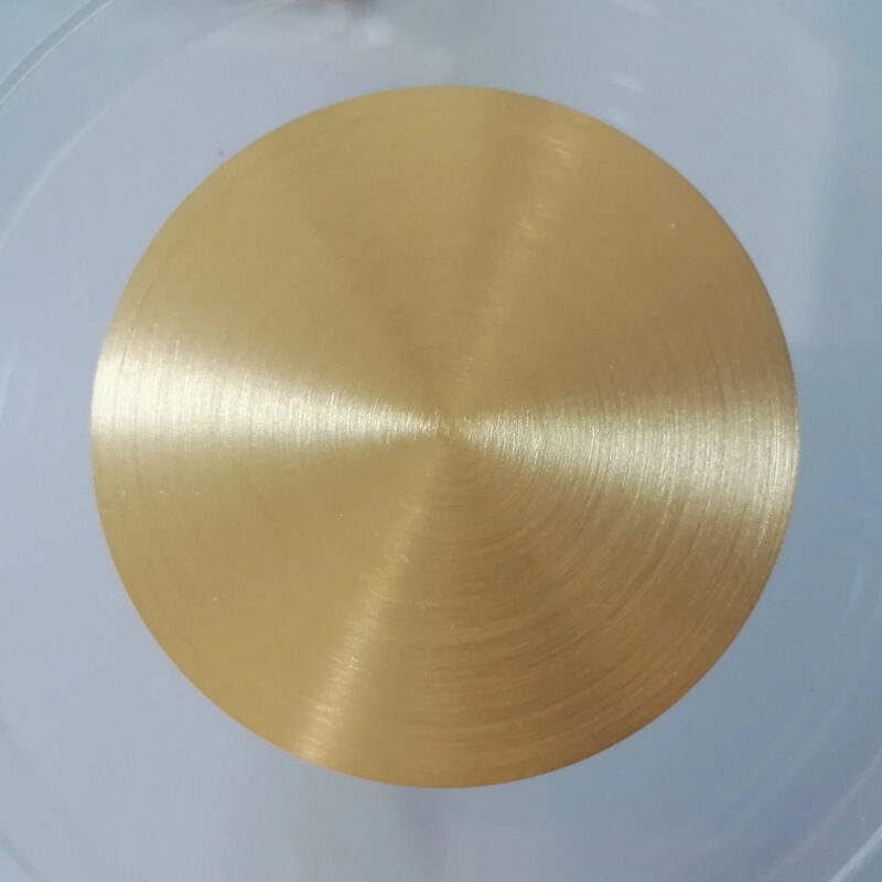
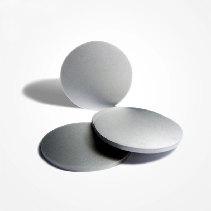
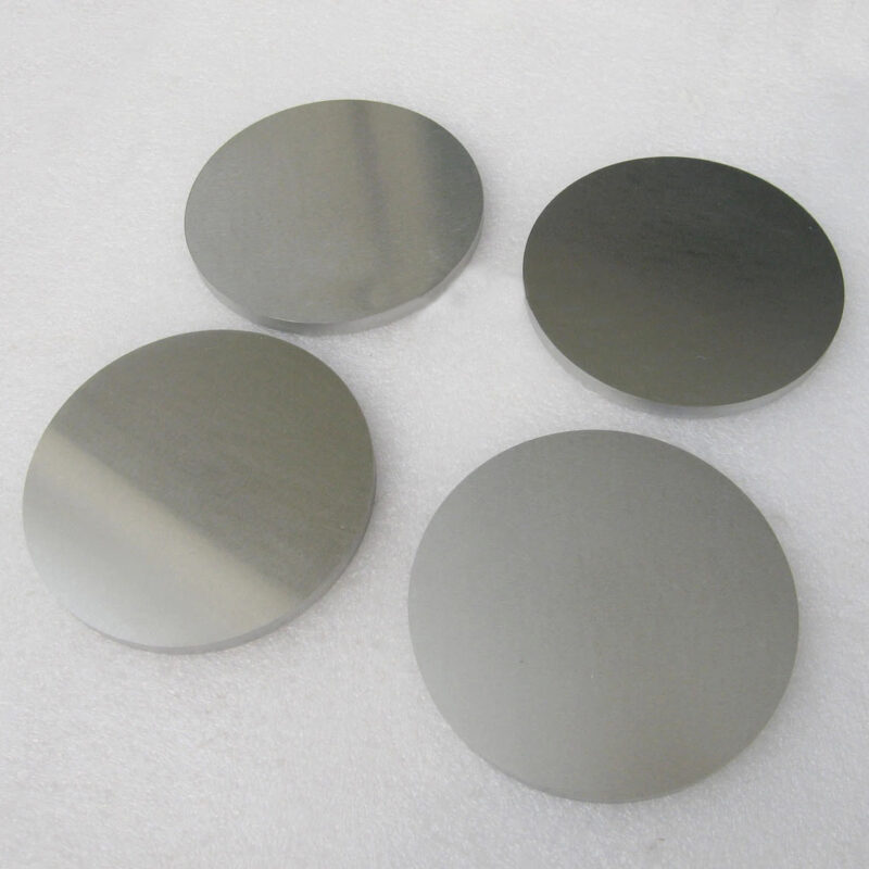
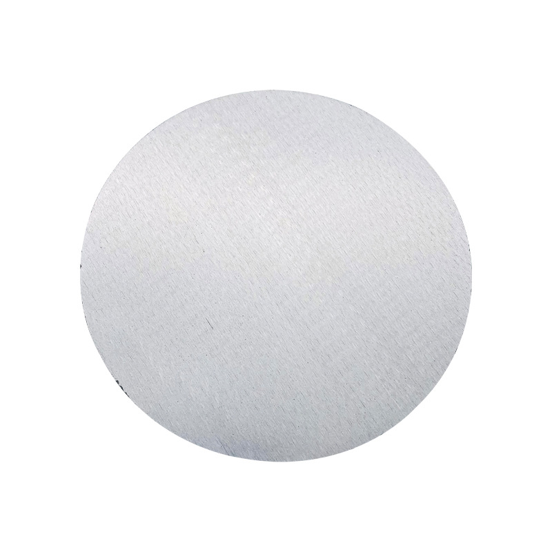
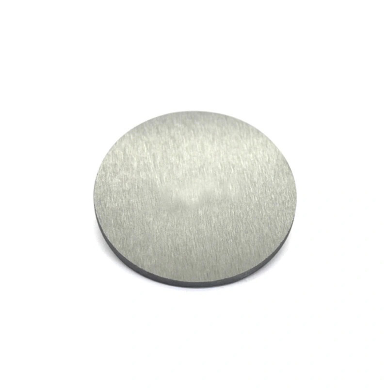
Cu2O (Cuprous Oxide) Sputtering Target
- Semiconductor Properties: Cu₂O is a p-type semiconductor with a direct bandgap, making it ideal for optoelectronic applications like solar cells and sensors.
- High Purity: High-purity Cu₂O sputtering targets are available to ensure efficient and precise deposition of thin films with minimal impurities.
- Environmentally Friendly: Cu₂O is a non-toxic, earth-abundant material, which makes it a sustainable choice for eco-friendly applications, especially in solar energy.
- Cost-effective: Compared to other materials, Cu₂O is affordable, making it attractive for large-scale applications such as photovoltaic cells.
Custom products or bulk orders, please contact us for competitive pricing!
- Satisfaction Guaranteed
- No Hassle Refunds
- Secure Payments
Description
| Material | Cu2O |
| Purity | 99.9% – 99.9999% / 3N 3N5 4N 4N5 5N 5N5 6N |
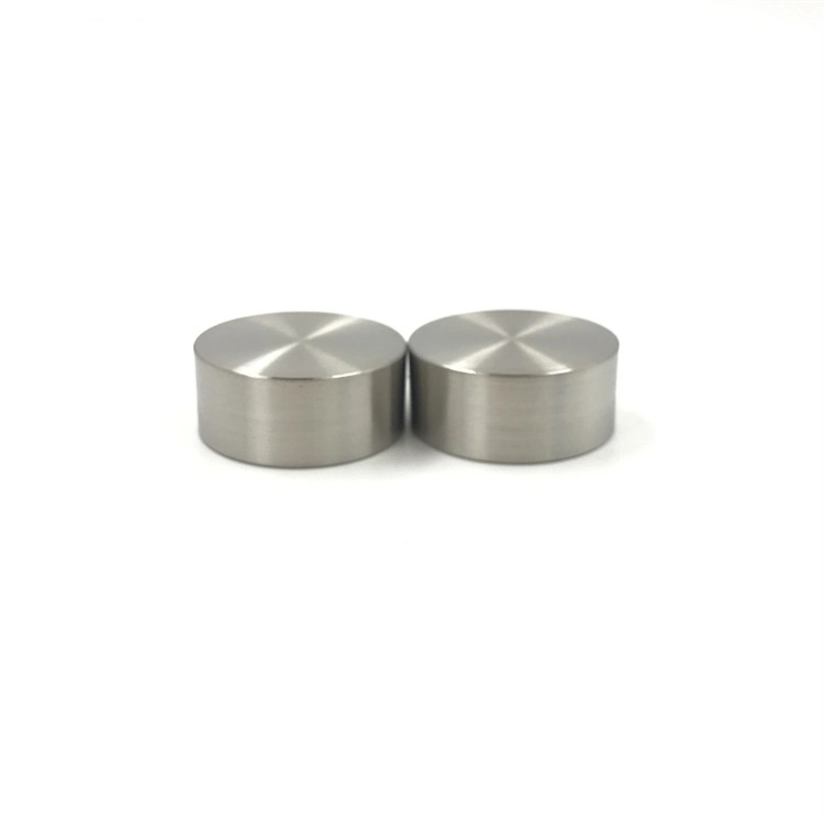
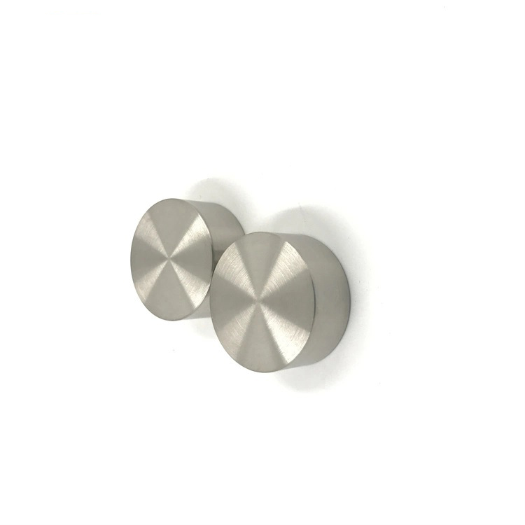
| Shape | disc, plate, sheet, rod, customized |
| Size | can be customized (contact us) |
| Package | vacuum bag or customer’s request |
| Place of Origin | China |
| MOQ | 1pcs |
| Supply Ability | 10000pcs per month |
| Lead Time | Qty: 1-100, Time: 3-10 days
Qty: >100, Time: to be negotiated |
Cu₂O (Cuprous Oxide) sputtering targets are widely used in thin-film applications such as solar cells, sensors, and optical coatings. Cu₂O is a p-type semiconductor with a relatively high optical transparency and a direct bandgap, making it suitable for various optoelectronic devices. It is also valued for its environmental friendliness and cost-effectiveness, making it a popular choice for sustainable energy applications.
Key Applications:
- Photovoltaic Cells: Cu₂O is often used in thin films for solar cells, where its direct bandgap (~2.1 eV) helps improve energy conversion efficiency.
- Gas Sensors: Thin films of Cu₂O are employed in gas-sensing applications due to their sensitivity to gases like carbon monoxide and hydrogen.
- Optoelectronic Devices: Cu₂O is also used in the production of thin-film transistors and diodes due to its semiconductor properties.
- Photocatalysis: Cu₂O thin films are used in photocatalytic applications, such as water splitting and degradation of organic pollutants under visible light.
Features of Cu₂O Sputtering Targets:
- Semiconductor Properties: Cu₂O is a p-type semiconductor with a direct bandgap, making it ideal for optoelectronic applications like solar cells and sensors.
- High Purity: High-purity Cu₂O sputtering targets are available to ensure efficient and precise deposition of thin films with minimal impurities.
- Environmentally Friendly: Cu₂O is a non-toxic, earth-abundant material, which makes it a sustainable choice for eco-friendly applications, especially in solar energy.
- Cost-effective: Compared to other materials, Cu₂O is affordable, making it attractive for large-scale applications such as photovoltaic cells.
Customization Options:
- Target Sizes and Shapes: Cu₂O sputtering targets are available in various shapes and sizes, allowing customization for different deposition systems.
- Purity Levels: Offered in high-purity levels to meet the stringent demands of electronic and optoelectronic applications.
- Bonding Services: Cu₂O targets can be bonded to backing plates to enhance thermal conductivity and mechanical stability during the sputtering process.
Cu₂O (Cuprous Oxide) sputtering targets from Tinsan Materials are perfect for solar cells, sensors, and optoelectronic devices. Cu₂O is a p-type semiconductor with a direct bandgap, ideal for sustainable energy and photocatalysis applications. Custom sizes and high-purity options available.
If you have specific requirements, such as dimensions, purity, or application details, please contact us to match your needs.
