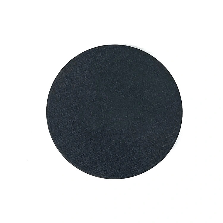
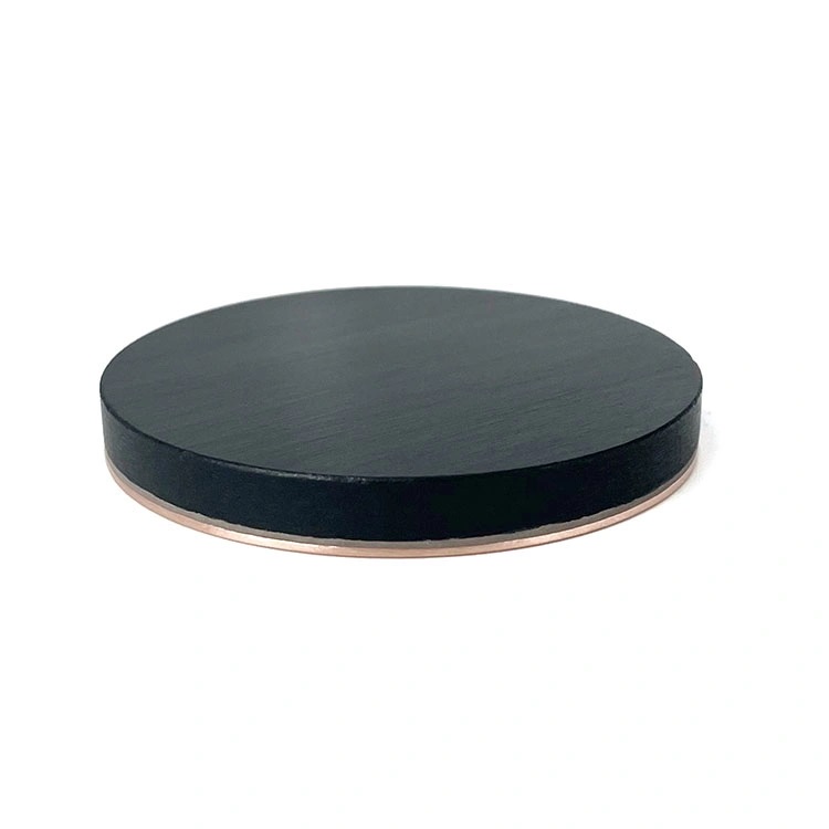
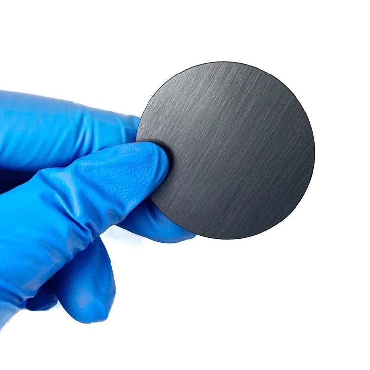
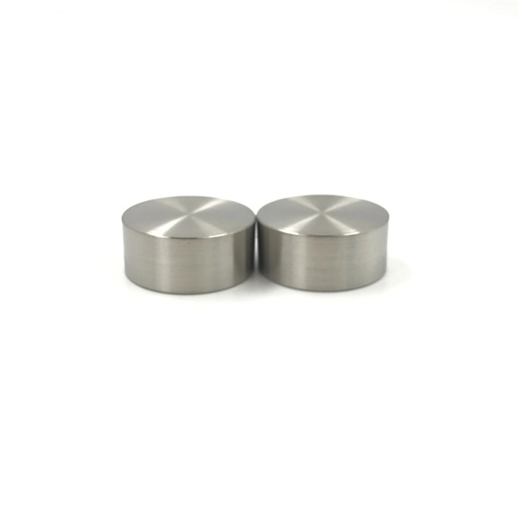
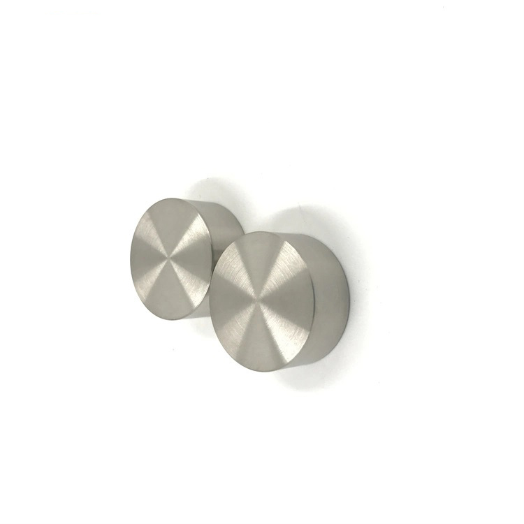
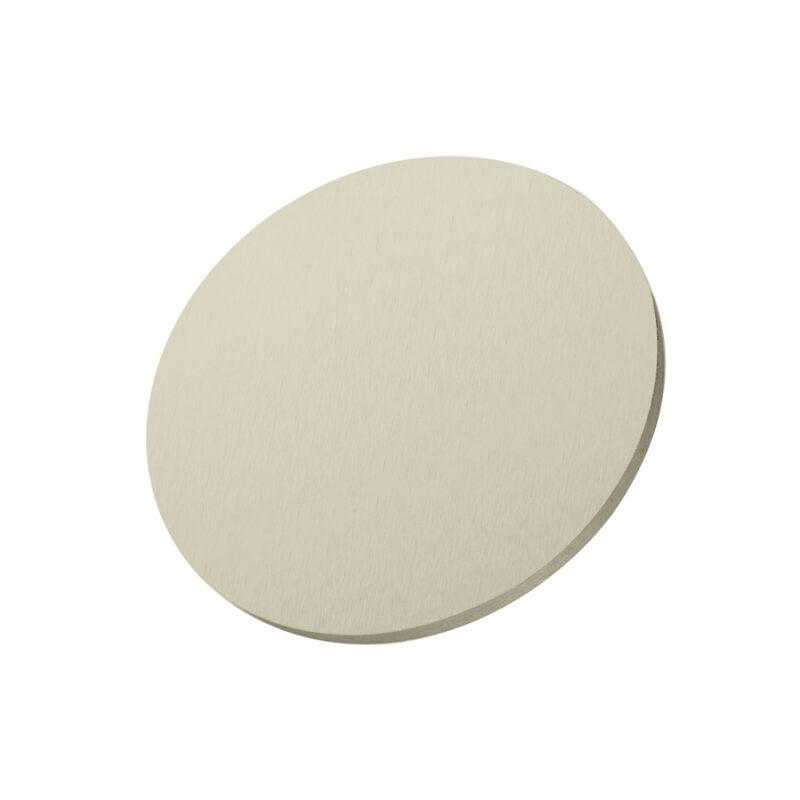
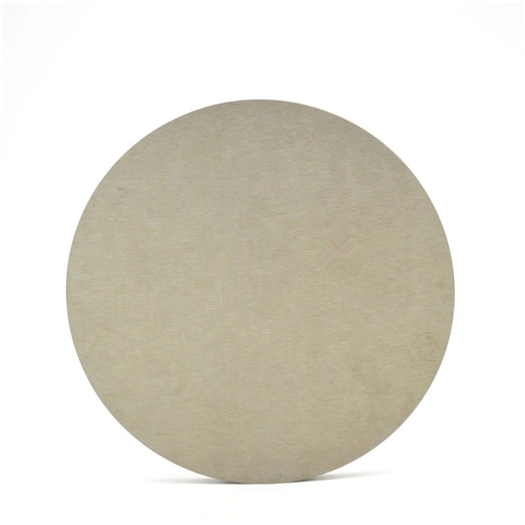
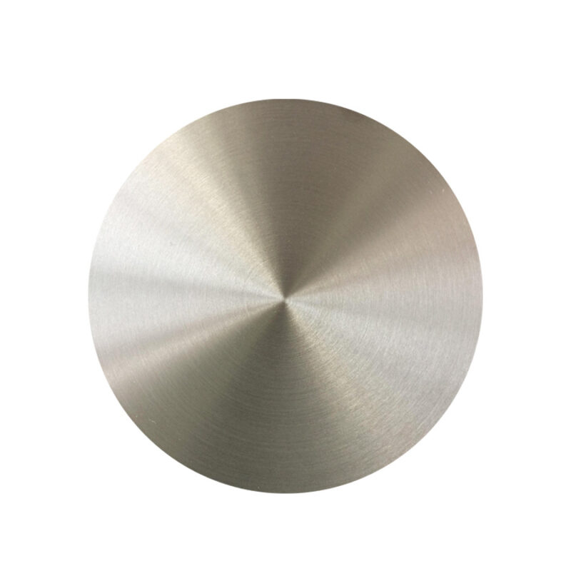
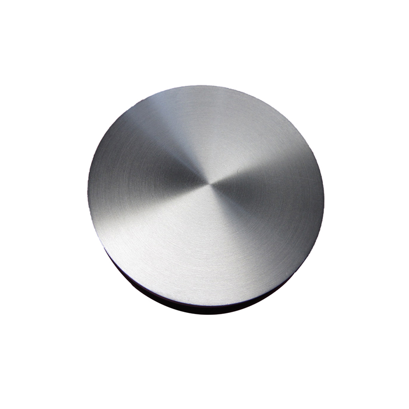
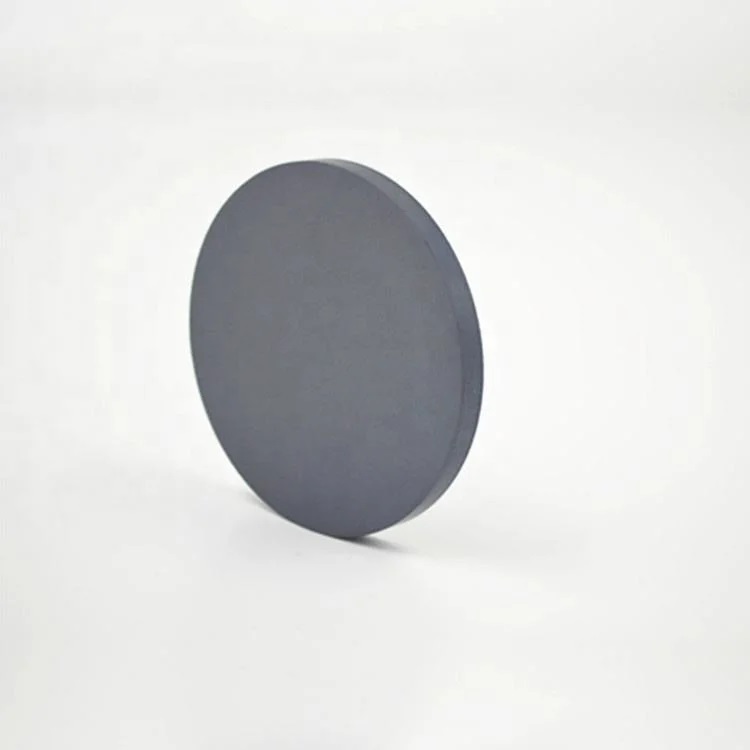
Cu2S (Copper Sulfide) Sputtering Target
- Semiconductor Properties: Cu₂S has p-type semiconductor properties, making it suitable for various electronic and photovoltaic applications.
- Good Optical Absorption: Cu₂S efficiently absorbs light, especially in the visible and near-infrared regions, making it ideal for solar cell applications.
- High Conductivity: Cu₂S exhibits good electrical conductivity, which is useful in applications that require conductive thin films.
- Thermal and Chemical Stability: Copper(I) Sulfide is thermally stable and resistant to certain chemicals, ensuring durability in harsh environments.
Custom products or bulk orders, please contact us for competitive pricing!
- Satisfaction Guaranteed
- No Hassle Refunds
- Secure Payments
Description
| Material | Copper Sulfide |
| Purity | 99.9% – 99.9999% / 3N 3N5 4N 4N5 5N 5N5 6N |
| Shape | disc, plate, sheet, rod, customized |
| Size | can be customized (contact us) |
| Package | vacuum bag or customer’s request |
| Place of Origin | China |
| MOQ | 1pcs |
| Supply Ability | 10000pcs per month |
| Lead Time | Qty: 1-100, Time: 3-10 days
Qty: >100, Time: to be negotiated |
Cu₂S (Copper(I) Sulfide) sputtering targets are used in thin-film deposition processes, particularly in the production of semiconductor devices, photovoltaics, and other electronic components. Copper(I) Sulfide is known for its unique electrical and optical properties, making it a valuable material in advanced technologies.
Key Applications:
- Photovoltaics: Cu₂S is widely used in thin-film solar cells, particularly in copper sulfide-based photovoltaic technologies, for its efficient light-absorbing properties.
- Semiconductor Devices: Cu₂S is a p-type semiconductor material, often used in the production of electronic components like diodes and transistors, as well as other semiconductor devices.
- Optoelectronic Devices: Due to its favorable optical properties, Cu₂S thin films are used in various optoelectronic applications, including sensors and detectors.
- Superionic Conductors: Cu₂S exhibits superionic conductivity, which can be leveraged in solid-state ionics and electrochemical devices, such as batteries and fuel cells.
- Catalysis: Cu₂S is also used as a catalyst in certain chemical reactions, making it valuable for industrial chemical processes.
Features of Cu₂S Sputtering Targets:
- Semiconductor Properties: Cu₂S has p-type semiconductor properties, making it suitable for various electronic and photovoltaic applications.
- Good Optical Absorption: Cu₂S efficiently absorbs light, especially in the visible and near-infrared regions, making it ideal for solar cell applications.
- High Conductivity: Cu₂S exhibits good electrical conductivity, which is useful in applications that require conductive thin films.
- Thermal and Chemical Stability: Copper(I) Sulfide is thermally stable and resistant to certain chemicals, ensuring durability in harsh environments.
Customization Options:
- Dimensions: Cu₂S sputtering targets are available in different shapes and sizes (discs, plates, and custom geometries) to fit various sputtering systems.
- Purity Levels: High-purity Cu₂S sputtering targets (up to 99.999%) are available for applications that require minimal impurities.
- Composition Control: Customization of the Cu ratio is possible to tailor the material’s electrical and optical properties for specific applications.
Cu₂S sputtering targets from Tinsan Materials offer excellent light absorption, semiconductor properties, and high conductivity for thin-film deposition in photovoltaics, optoelectronics, and semiconductor devices. Custom sizes and high-purity targets available.
If you have specific requirements, such as dimensions, purity, or application details, please contact us to match your needs.
