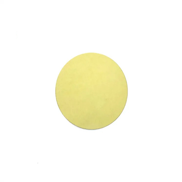
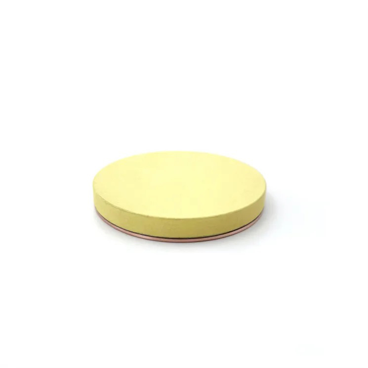
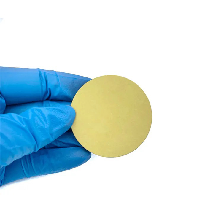
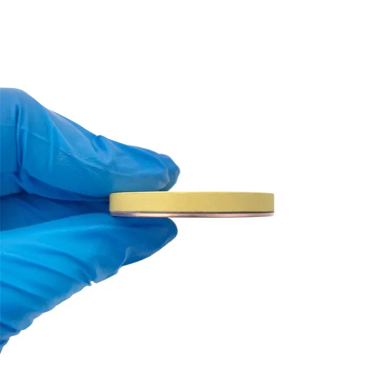
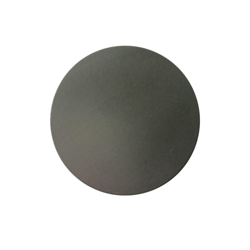
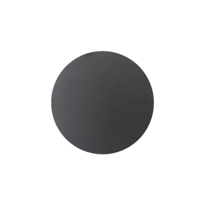
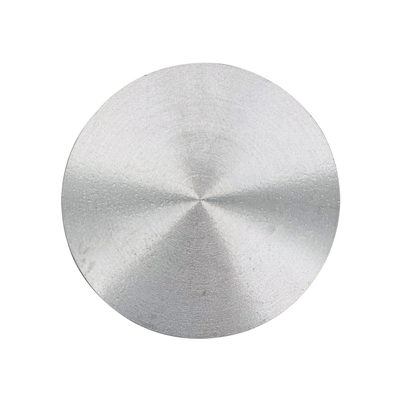
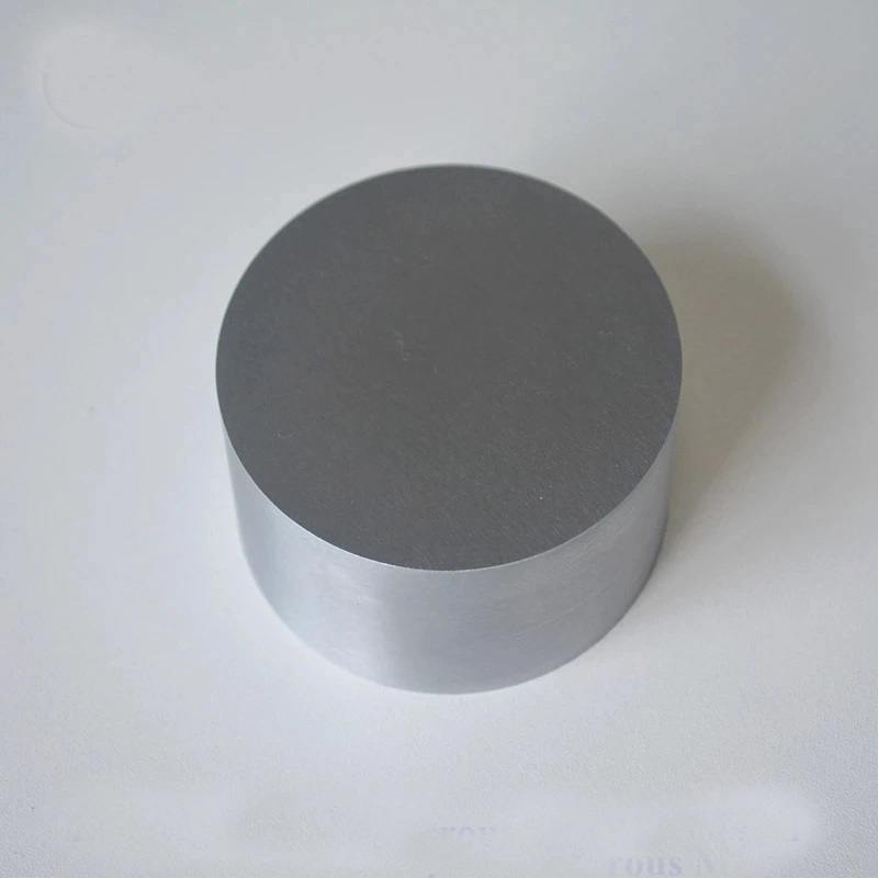
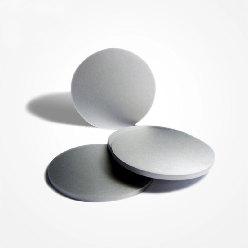
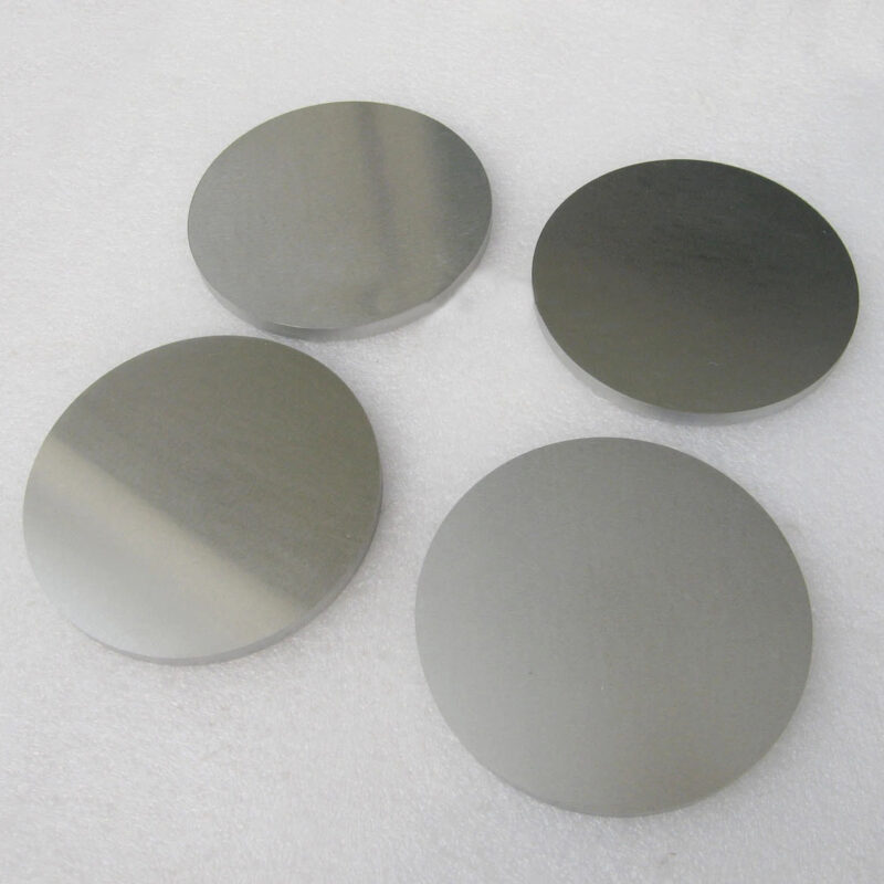
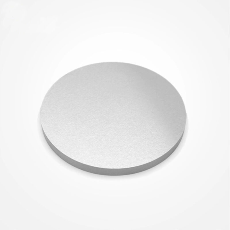
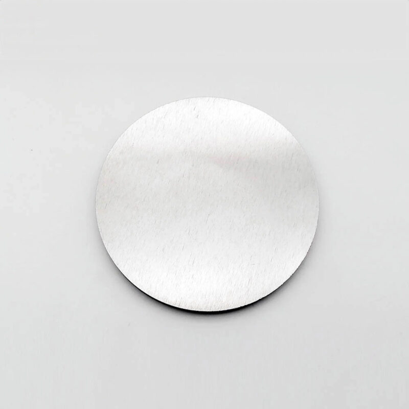
In2O3 (Indium Oxide) Sputtering Target
- High Transparency: In2O3 is optically transparent in the visible range, making it ideal for transparent electrode applications.
- Good Conductivity: Indium oxide offers good electrical conductivity, which can be optimized for use in optoelectronic devices and transparent electrodes.
- Chemical Stability: In2O3 is chemically stable, ensuring long-term durability of thin films in harsh environments.
- Wide Bandgap: The wide bandgap of indium oxide allows it to function effectively in optoelectronic and sensor applications, especially in high-temperature conditions.
- Custom Purity Levels: In2O3 sputtering targets are available in high purities (up to 99.999%) to ensure the deposition of high-quality, defect-free films.
Custom products or bulk orders, please contact us for competitive pricing!
- Satisfaction Guaranteed
- No Hassle Refunds
- Secure Payments
Description
| Material | In2O3 |
| Purity | 99.9% – 99.99999% / 3N 3N5 4N 4N5 5N 5N5 6N 6N5 7N |
| Shape | disc, plate, sheet, rod, customized |
| Size | can be customized (contact us) |
| Package | vacuum bag or customer’s request |
| Place of Origin | China |
| MOQ | 1pcs |
| Supply Ability | 10000pcs per month |
| Lead Time | Qty: 1-100, Time: 3-10 days
Qty: >100, Time: to be negotiated |
Indium Oxide (In2O3) sputtering targets are used to deposit thin films of indium oxide in various applications, especially in the fields of electronics, optics, and sensors. Indium oxide is a transparent conducting oxide (TCO), which is commonly used for applications requiring high electrical conductivity and transparency in the visible spectrum. It is also known for its chemical stability, making it suitable for diverse environments.
Key Applications:
- Optoelectronics: In2O3 thin films are used in optoelectronic devices like photodetectors, light-emitting diodes (LEDs), and infrared detectors due to their transparent conductive properties.
- Thin-Film Transistors (TFTs): Indium oxide is applied in TFTs as a transparent semiconductor, particularly in display technologies such as liquid crystal displays (LCDs) and OLEDs.
- Touch Panels and Displays: In2O3 is used in the manufacture of transparent electrodes for touchscreens and flat-panel displays.
- Photovoltaics: In2O3 sputtering targets are used in solar cells, where they form transparent conductive layers that allow light to pass through while conducting electricity.
- Gas Sensors: Indium oxide films are sensitive to gases, making them suitable for use in sensors detecting pollutants such as ozone, nitrogen dioxide, and ethanol.
Features of In2O3 Sputtering Targets:
- High Transparency: In2O3 is optically transparent in the visible range, making it ideal for transparent electrode applications.
- Good Conductivity: Indium oxide offers good electrical conductivity, which can be optimized for use in optoelectronic devices and transparent electrodes.
- Chemical Stability: In2O3 is chemically stable, ensuring long-term durability of thin films in harsh environments.
- Wide Bandgap: The wide bandgap of indium oxide allows it to function effectively in optoelectronic and sensor applications, especially in high-temperature conditions.
- Custom Purity Levels: In2O3 sputtering targets are available in high purities (up to 99.999%) to ensure the deposition of high-quality, defect-free films.
Customization Options:
- Dimensions: In2O3 sputtering targets are available in a range of sizes and geometries, including planar and cylindrical designs, customized for different sputtering systems.
- Purity: High-purity In2O3 targets are available, ensuring the production of films with minimal contamination, which is crucial for electronic and optical applications.
- Target Bonding: Targets can be bonded to backing plates to enhance thermal conductivity and improve sputtering efficiency, ensuring long-lasting performance.
In2O3 (Indium Oxide) sputtering targets from Tinsan Materials are ideal for transparent conductive films in optoelectronics, touch panels, TFTs, and gas sensors. High-purity targets available for optimal thin-film deposition.
If you have specific requirements, such as dimensions, purity, or application details, please contact us to match your needs.
