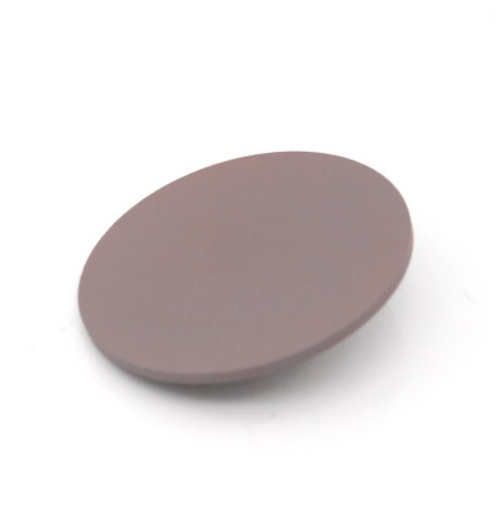
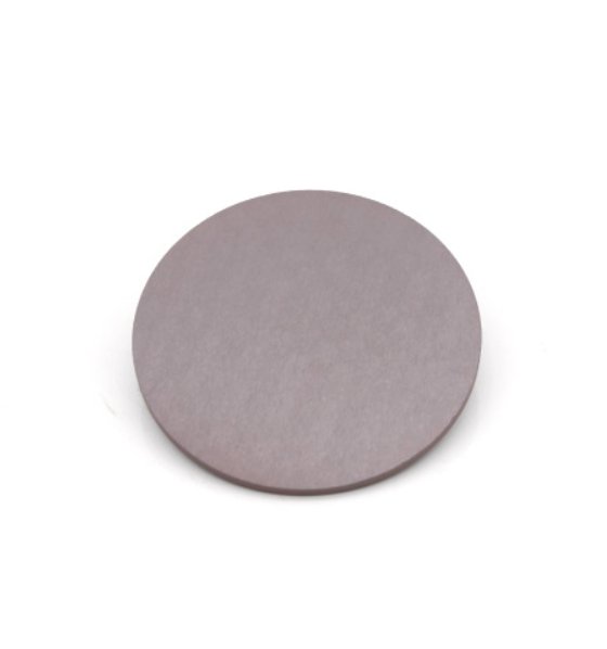
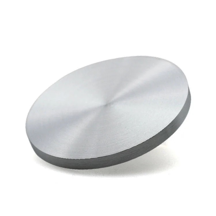
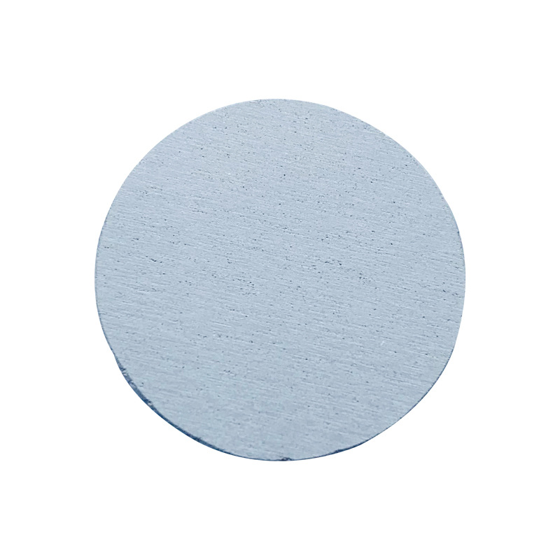
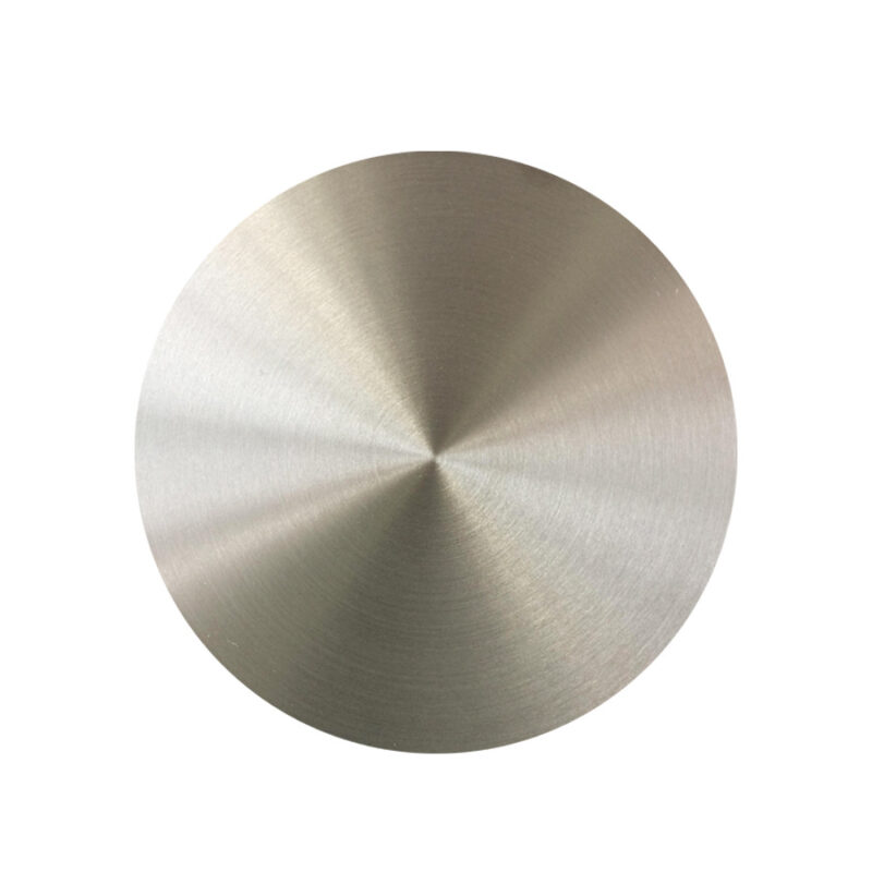
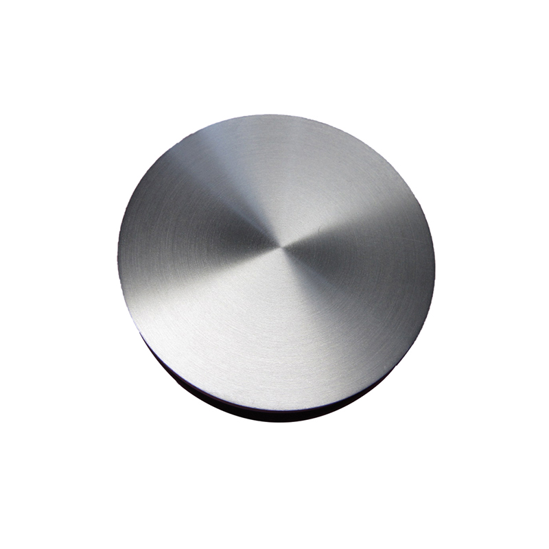
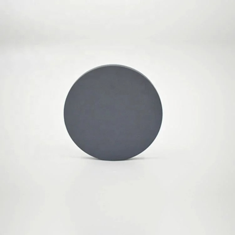
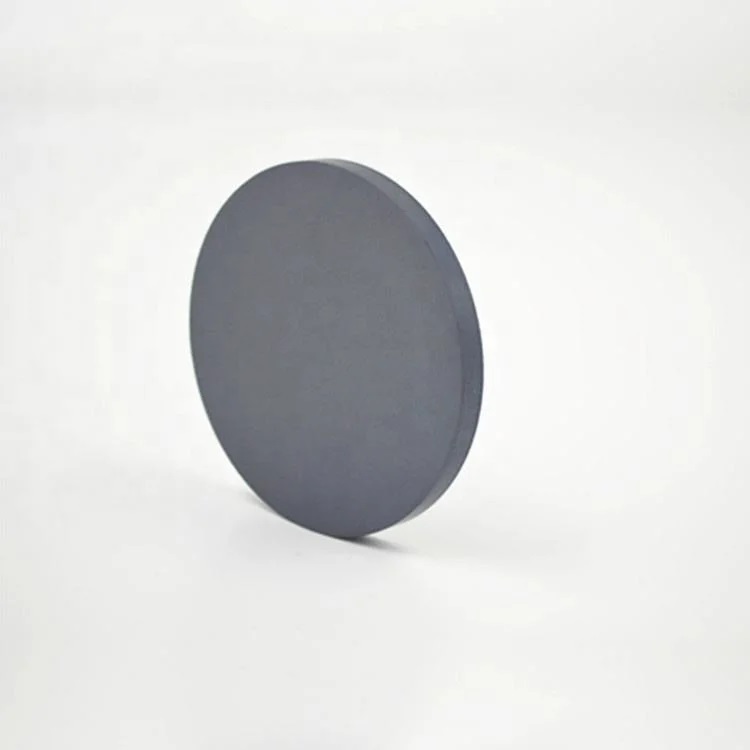
In2S3 (Indium Sulfide) Sputtering Targets
- High Optical Transparency: Suitable for applications requiring minimal light absorption.
- Wide Bandgap: Excellent for photovoltaic and semiconductor applications.
- Low Toxicity: Eco-friendly alternative to cadmium-based materials.
- Customizable Specifications: Tailored for specific deposition processes and applications.
- High Purity: Ensures consistent film quality and enhanced device performance.
Custom products or bulk orders, please contact us for competitive pricing!
- Satisfaction Guaranteed
- No Hassle Refunds
- Secure Payments
Description
| Material | Indium Sulfide (In₂S₃) |
| Purity | 99.9% – 99.9999% / 3N 3N5 4N 4N5 5N 5N5 6N |
| Shape | disc, plate, sheet, rod, customized |
| Size | can be customized (contact us) |
| Package | vacuum bag or customer’s request |
| Place of Origin | China |
| MOQ | 1pcs |
| Supply Ability | 10000pcs per month |
| Lead Time | Qty: 1-100, Time: 3-10 days
Qty: >100, Time: to be negotiated |
Indium Sulfide (In₂S₃) sputtering targets are widely utilized for thin-film deposition in optoelectronic and photovoltaic applications. This nontoxic alternative to cadmium-based materials is known for its excellent optical and electrical properties, making it a popular choice in fabricating buffer layers for solar cells, sensors, and other semiconductor devices. Its high transparency and wide bandgap enable it to meet the stringent requirements of advanced electronic applications.
Key Applications
- Photovoltaics: Ideal for buffer layers in CIGS (Copper Indium Gallium Selenide) solar cells.
- Optoelectronics: Utilized in light sensors, LEDs, and display technologies.
- Thin-film Semiconductors: Suitable for transparent conductive films.
- Energy Storage: Research applications in thin-film batteries and capacitors.
Features and Benefits
- High Optical Transparency: Suitable for applications requiring minimal light absorption.
- Wide Bandgap: Excellent for photovoltaic and semiconductor applications.
- Low Toxicity: Eco-friendly alternative to cadmium-based materials.
- Customizable Specifications: Tailored for specific deposition processes and applications.
- High Purity: Ensures consistent film quality and enhanced device performance.
Specifications
- Purity: ≥ 99.9% for superior thin-film deposition.
- Density: Optimized for uniform sputtering rates.
- Shape: Disc, rectangular, or custom geometries available.
- Dimensions: Wide range of sizes to fit various sputtering equipment.
Customization Options
- Composition Modifications: Tailored for specific electrical or optical properties.
- Backing Plates: Available for improved thermal management during deposition.
- Dimensions: Custom shapes and sizes to meet specific sputtering requirements.
Reach out to us for more information on Indium Sulfide (In₂S₃) sputtering targets. Our team provides expert advice, competitive pricing, and tailored solutions to meet your project needs.
If you have specific requirements, such as dimensions, purity, or application details, please contact us to match your needs.
