Monocrystalline Silicon Wafers (Intrinsic/N-Type/P-Type)
- Diameter Choices: 2″ to 12″ (or custom sizes).
- Doping Concentration: Custom doping profiles for N-type and P-type wafers.
- Thickness Variability: From ultra-thin wafers to thick substrates.
- Crystal Orientation: Standard orientations include <100>, <111>, <110>, with custom orientations available.
- Flat & Edge Treatment: Rounded, chamfered, or custom edge profiles.
- Surface Finishing:
- SSP (Single-Side Polished) or DSP (Double-Side Polished).
- Oxide coating, etched surfaces, or epitaxial layers upon request.
Custom products or bulk orders, please contact us for competitive pricing!
- Satisfaction Guaranteed
- No Hassle Refunds
- Secure Payments
Description
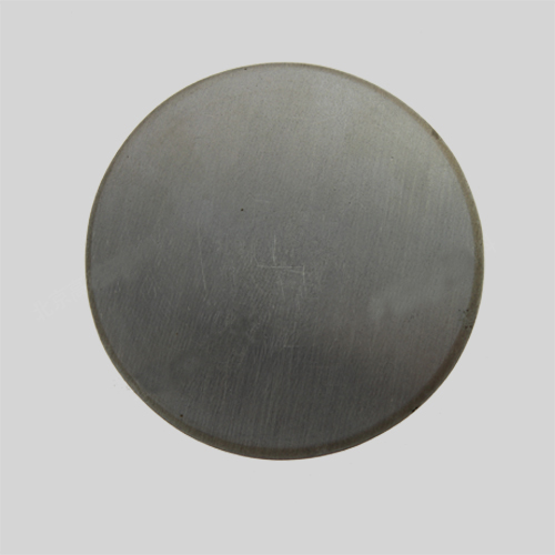
Monocrystalline silicon wafers are high-purity silicon substrates widely used in semiconductor manufacturing, MEMS (Micro-Electro-Mechanical Systems), infrared optics, solar cells, and power electronics. These wafers are available in Intrinsic (Undoped), N-Type, and P-Type doping types, each catering to specific applications.
- Intrinsic Silicon (Undoped Si): High-purity silicon with no intentional doping, ideal for optical and research applications.
- N-Type Silicon: Doped with elements such as Phosphorus (P), Antimony (Sb), or Arsenic (As) to create excess free electrons, enhancing conductivity.
- P-Type Silicon: Doped with Boron (B) or Gallium (Ga) to create holes as charge carriers, commonly used in semiconductor devices and power applications.
Wafers from Tinsan Materials are available in various sizes, orientations, resistivities, and surface finishes to meet diverse industry needs.
Specifications & Properties
| Material Type | Intrinsic, N-Type (P, Sb, As), P-Type (B, Ga) |
| Diameter | 2″ (50.8mm) – 12″ (300mm) |
| Thickness | 100µm – 725µm (Customizable) |
| Crystal Orientation | <100>, <111>, <110> |
| Resistivity | 0.001 Ω·cm – 1000 Ω·cm |
| Doping Concentration | Customizable based on application |
| Surface Finish | Single-side polished (SSP) or Double-side polished (DSP) |
| Edge Treatment | Rounded edges, chamfered edges |
| Flatness & TTV | SEMI Standard Compliance |
| Oxide Coating | Available upon request |
These specifications can be tailored to meet your specific application requirements.
Doping Types & Applications
1. Intrinsic Silicon (Undoped Si)
- Features: High purity, excellent infrared transparency, minimal free charge carriers.
- Applications: Infrared optics, sensors, high-precision research, and experimental physics.
2. N-Type Silicon
- Dopants: Phosphorus (P), Antimony (Sb), Arsenic (As).
- Electrical Properties: Excess electrons provide high conductivity, low resistance.
- Applications:
- Semiconductor devices (MOSFETs, ICs, transistors).
- High-speed electronics.
- Solar cell applications requiring longer carrier lifetimes.
3. P-Type Silicon
- Dopants: Boron (B), Gallium (Ga).
- Electrical Properties: Hole carriers dominate, enabling controlled conduction.
- Applications:
- Power semiconductor devices.
- Sensor and MEMS devices.
- CMOS technology and integrated circuits.
Key Advantages
- High Purity & Uniformity – Ensures consistent device performance.
- Customizable Electrical & Mechanical Properties – Adjustable resistivity, thickness, and doping levels.
- Excellent Surface Quality – Polished surfaces for superior device fabrication.
- Compatible with Semiconductor Processing – High-quality wafers for advanced photolithography and etching processes.
- Infrared Transparency (for intrinsic Si) – Ideal for IR optics applications.
Applications
- Semiconductor Industry – Used in ICs, transistors, diodes, and photonic devices.
- MEMS & Sensor Technology – High-precision silicon substrates for micro-electromechanical systems.
- Solar Energy – High-efficiency monocrystalline silicon solar cells.
- Infrared Optics – Silicon windows and lenses for IR imaging and spectroscopy.
- Power Electronics – P-type wafers used in IGBTs, MOSFETs, and rectifiers.
- Scientific Research – Fundamental material for advanced material science and physics research.
Customization Options
To meet specific project requirements, we offer fully customizable monocrystalline silicon wafers with:
- Diameter Choices: 2″ to 12″ (or custom sizes).
- Doping Concentration: Custom doping profiles for N-type and P-type wafers.
- Thickness Variability: From ultra-thin wafers to thick substrates.
- Crystal Orientation: Standard orientations include <100>, <111>, <110>, with custom orientations available.
- Flat & Edge Treatment: Rounded, chamfered, or custom edge profiles.
- Surface Finishing:
- SSP (Single-Side Polished) or DSP (Double-Side Polished).
- Oxide coating, etched surfaces, or epitaxial layers upon request.
We ensure each wafer meets strict industry standards and provides exceptional reliability in critical applications.
Quality & Certifications
Our silicon wafers are produced under strict quality control to meet global semiconductor industry standards:
- SEMI Standard Compliant – Precision manufacturing to industry specifications.
- ISO 9001 Certified – Quality management system ensuring consistency.
- RoHS & REACH Compliance – Environmentally safe, free from hazardous substances.
- Cleanroom Packaging – Contamination-free, secure packaging for shipment.
Ordering & Contact Information
We offer flexible MOQ (Minimum Order Quantity) and competitive pricing. Our wafers are packaged in Class 100 cleanroom environments and shipped worldwide. For custom orders or technical inquiries, please contact us for a detailed consultation!

