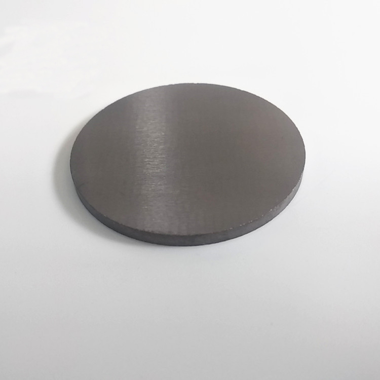
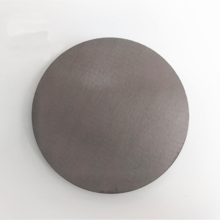
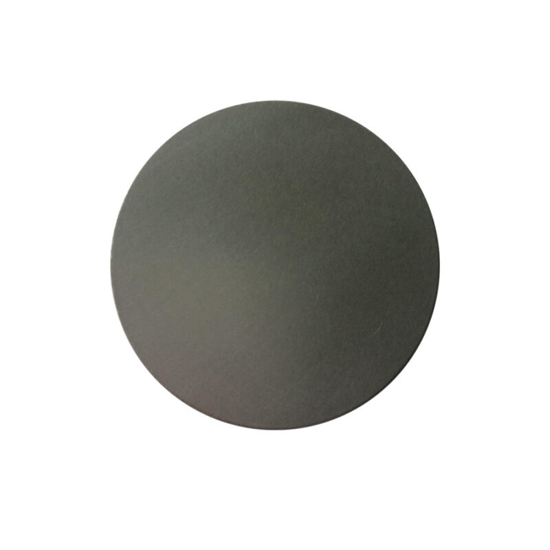
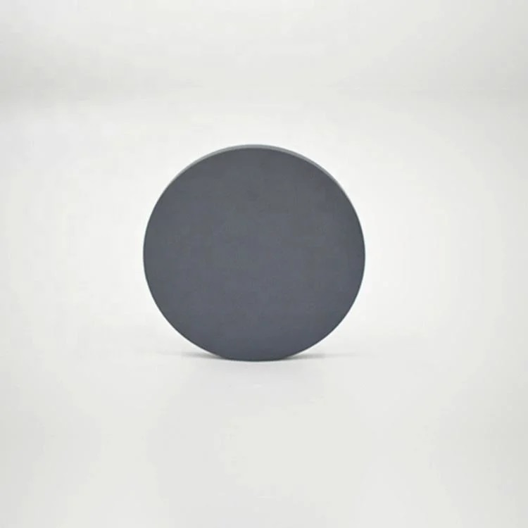
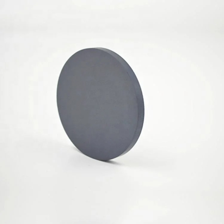
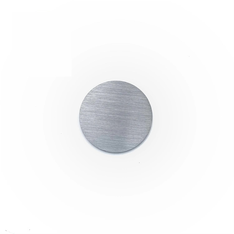
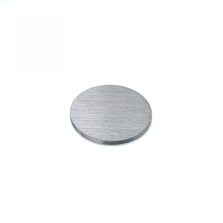
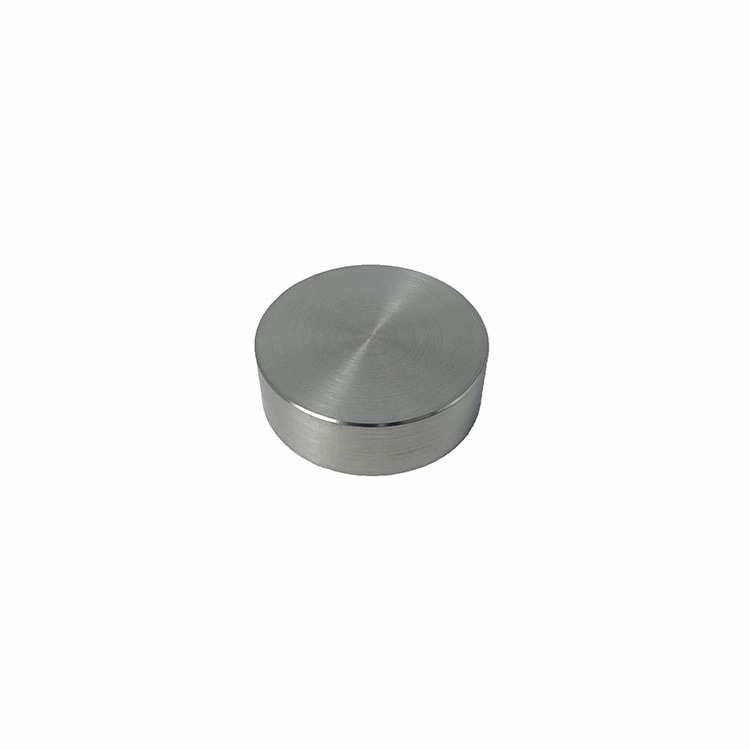
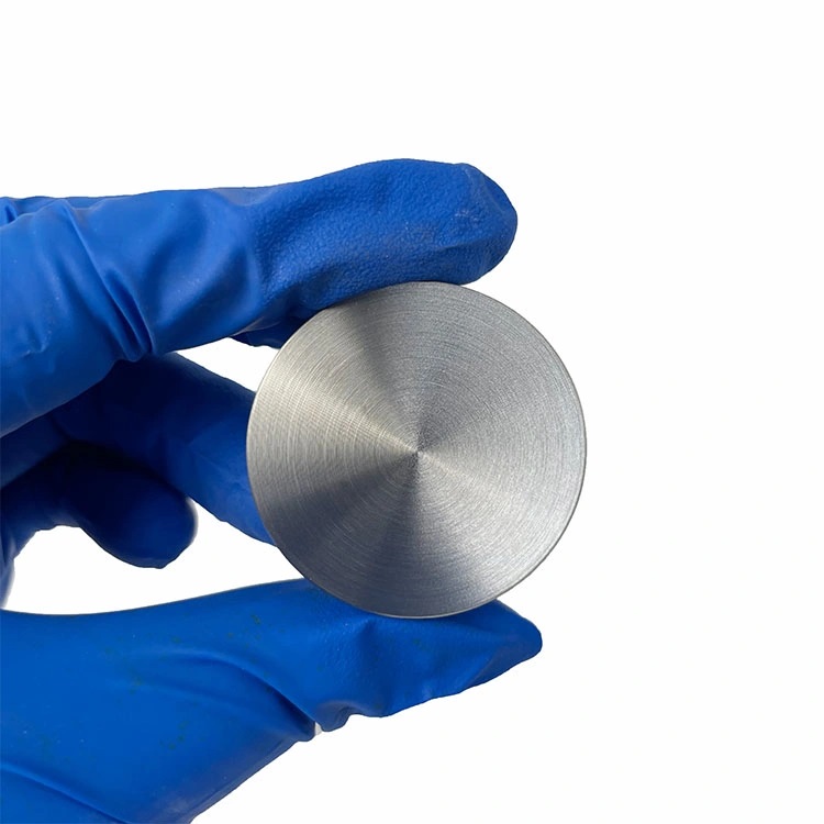
MoSe2 (Molybdenum Diselenide) Sputtering Targets
- High Purity: Ensures superior thin-film quality and device performance.
- Layered Structure: Facilitates easy exfoliation and 2D material synthesis.
- Stable Chemical Composition: Provides consistent results across various deposition processes.
- Excellent Optical and Electrical Properties: Ideal for advanced electronics and optoelectronics.
- Custom Configurations: Available in tailored sizes, shapes, and thicknesses for specific requirements.
Custom products or bulk orders, please contact us for competitive pricing!
- Satisfaction Guaranteed
- No Hassle Refunds
- Secure Payments
Description
| Material | Molybdenum Diselenide (MoSe₂) |
| Purity | 99.9% – 99.9999% / 3N 3N5 4N 4N5 5N 5N5 6N |
| Shape | disc, plate, sheet, rod, customized |
| Size | can be customized (contact us) |
| Package | vacuum bag or customer’s request |
| Place of Origin | China |
| MOQ | 1pcs |
| Supply Ability | 10000pcs per month |
| Lead Time | Qty: 1-100, Time: 3-10 days
Qty: >100, Time: to be negotiated |
Molybdenum Diselenide (MoSe₂) sputtering targets are high-quality materials engineered for thin-film deposition in advanced electronics, photonics, and energy storage systems. With a layered structure and excellent semiconducting properties, MoSe₂ is a key material in the development of 2D materials, optoelectronic devices, and photovoltaic technologies.
Key Applications
- 2D Materials Research: Used in the fabrication of ultra-thin, high-performance layers for next-generation electronics.
- Optoelectronics: Essential for photodetectors, light-emitting diodes (LEDs), and modulators.
- Energy Conversion and Storage: Suitable for applications in solar cells and supercapacitors.
- Semiconductors: Provides excellent properties for transistors and integrated circuits.
- Photovoltaics: Enhances the efficiency of solar energy harvesting systems.
Features and Benefits
- High Purity: Ensures superior thin-film quality and device performance.
- Layered Structure: Facilitates easy exfoliation and 2D material synthesis.
- Stable Chemical Composition: Provides consistent results across various deposition processes.
- Excellent Optical and Electrical Properties: Ideal for advanced electronics and optoelectronics.
- Custom Configurations: Available in tailored sizes, shapes, and thicknesses for specific requirements.
Specifications
- Purity: ≥ 99.95%, ensuring minimal contamination in thin-film applications.
- Density: Optimized for uniform deposition and high material utilization.
- Dimensions: Customizable to fit a wide range of sputtering systems.
- Forms: Available in discs, plates, or other geometries as needed.
- Surface Finish: Polished to a smooth surface for consistent sputtering performance.
Customization Options
- Size and Shape Customization: Adaptable to specific equipment and process needs.
- Bonding Services: Compatible backing plates for improved thermal management.
- Special Packaging: Designed for safe handling and transportation.
- Material Variations: Compositional adjustments for specialized applications.
Discover high-quality Molybdenum Diselenide (MoSe₂) sputtering targets tailored to your thin-film deposition projects. Contact us for expert consultation, custom solutions, and prompt delivery.
