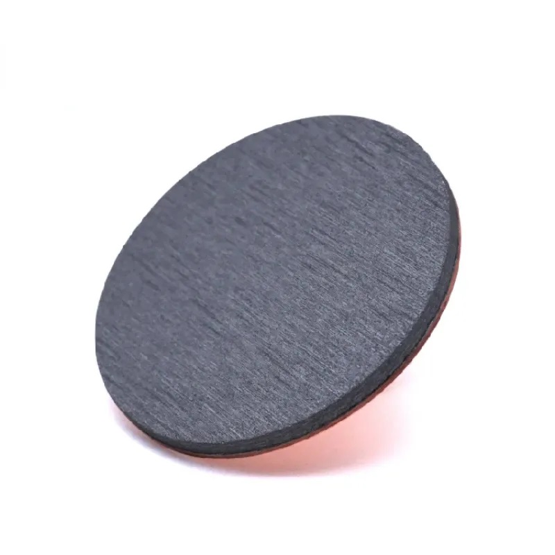
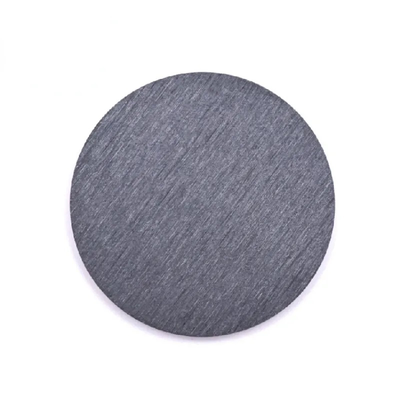
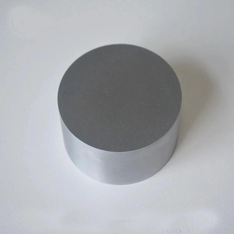
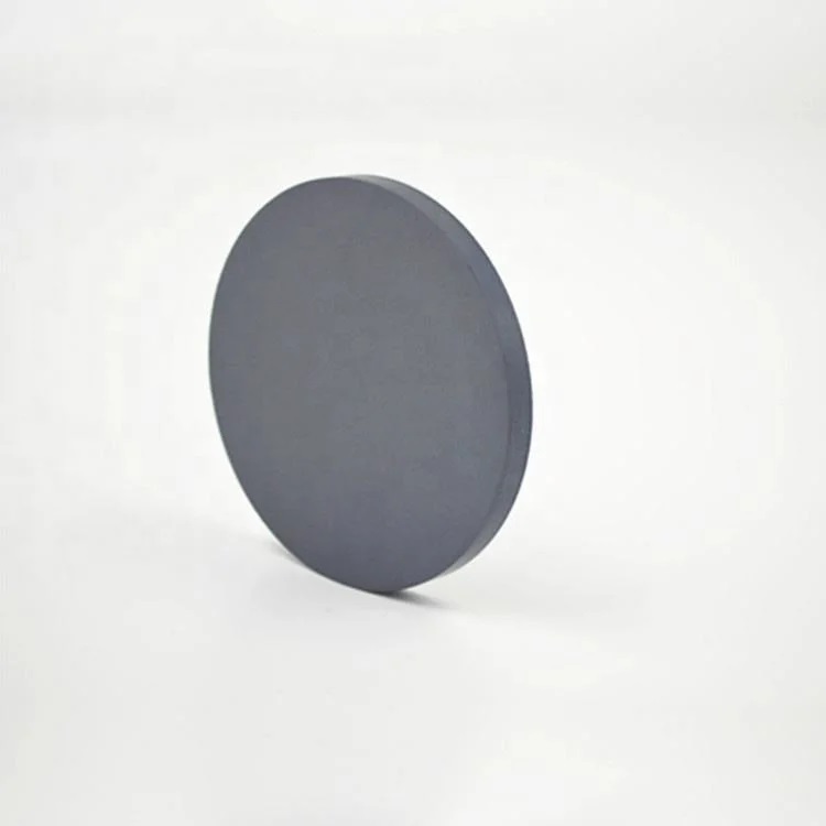
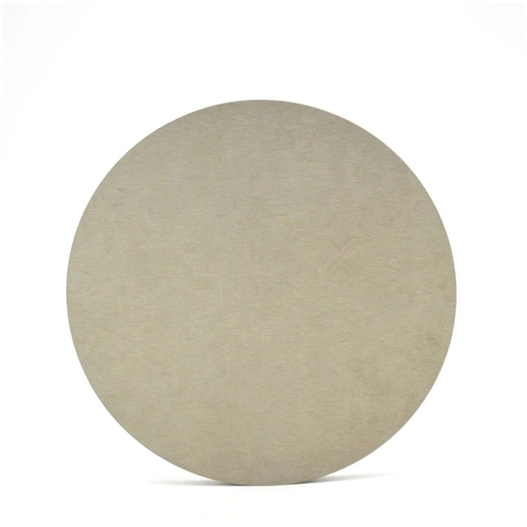
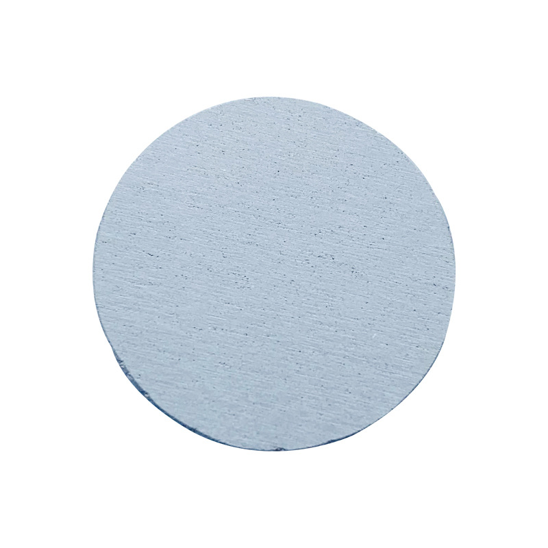
Sb2Se3 (Antimony Selenide) Sputtering Target
- High Absorption Coefficient: Sb₂Se₃ has a high absorption coefficient, which makes it effective for thin-film solar cells and light-harvesting applications.
- Bandgap: The material has a bandgap around 1.1 to 1.3 eV, ideal for photovoltaic devices aimed at capturing sunlight efficiently.
- Non-Toxic and Earth-Abundant: Sb₂Se₃ offers an environmentally friendlier and more sustainable alternative to other thin-film materials like cadmium-based compounds.
- Stable Crystal Structure: Sb₂Se₃ thin films exhibit a stable orthorhombic crystal structure, which contributes to their robustness in various electronic and energy-related applications.
Custom products or bulk orders, please contact us for competitive pricing!
- Satisfaction Guaranteed
- No Hassle Refunds
- Secure Payments
Description
| Material | Sb2Se3 |
| Purity | 99.9% – 99.9999% / 3N 3N5 4N 4N5 5N 5N5 6N |
| Shape | disc, plate, sheet, rod, customized |
| Size | can be customized (contact us) |
| Package | vacuum bag or customer’s request |
| Place of Origin | China |
| MOQ | 1pcs |
| Supply Ability | 10000pcs per month |
| Lead Time | Qty: 1-100, Time: 3-10 days
Qty: >100, Time: to be negotiated |
Antimony Selenide (Sb₂Se₃) sputtering targets are used in thin film deposition for a range of optoelectronic, photovoltaic, and thermoelectric applications. Sb₂Se₃ has attracted significant attention for its application in next-generation solar cells due to its favorable optical properties and suitable bandgap for sunlight absorption.
Key Applications:
- Photovoltaics: Sb₂Se₃ is a promising material for thin-film solar cells, offering high absorption efficiency and potential as an alternative to traditional materials like silicon and cadmium telluride (CdTe).
- Thermoelectrics: Sb₂Se₃ thin films are also used in thermoelectric devices, where they help convert temperature differences into electrical voltage due to their unique semiconducting properties.
- Optoelectronics: Sb₂Se₃ films can be used in photodetectors and other optoelectronic devices for infrared sensing, benefiting from their broad absorption spectrum.
- Thin Film Transistors (TFTs): Sb₂Se₃ thin films are explored in the development of TFTs due to their semiconducting nature and compatibility with flexible electronics.
Features of Sb₂Se₃ Sputtering Targets:
- High Absorption Coefficient: Sb₂Se₃ has a high absorption coefficient, which makes it effective for thin-film solar cells and light-harvesting applications.
- Bandgap: The material has a bandgap around 1.1 to 1.3 eV, ideal for photovoltaic devices aimed at capturing sunlight efficiently.
- Non-Toxic and Earth-Abundant: Sb₂Se₃ offers an environmentally friendlier and more sustainable alternative to other thin-film materials like cadmium-based compounds.
- Stable Crystal Structure: Sb₂Se₃ thin films exhibit a stable orthorhombic crystal structure, which contributes to their robustness in various electronic and energy-related applications.
Customization Options:
- Target Dimensions: Available in a variety of diameters, thicknesses, and shapes tailored to specific sputtering systems.
- Purity Levels: High-purity Sb₂Se₃ targets are provided to ensure quality deposition and superior thin-film performance.
- Bonding Services: Targets can be bonded to backing plates to ensure thermal conductivity and stability during sputtering.
Tinsan Materials offers Sb₂Se₃ (Antimony Selenide) sputtering targets for thin film deposition in photovoltaics, thermoelectrics, and optoelectronics. Known for its high absorption efficiency and suitable bandgap, Sb₂Se₃ is ideal for next-generation solar cells and thermoelectric applications.
If you have specific requirements, such as dimensions, purity, or application details, please contact us to match your needs.
