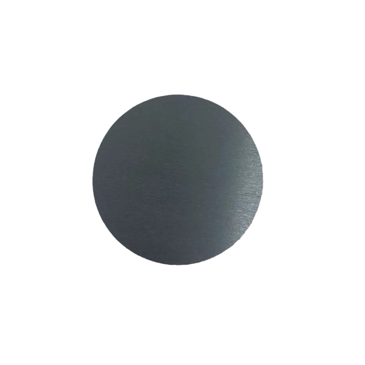
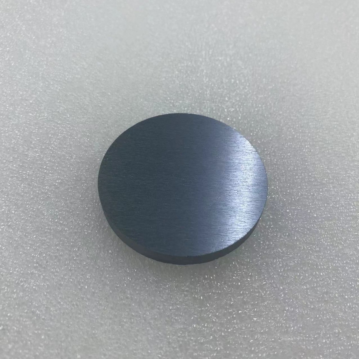
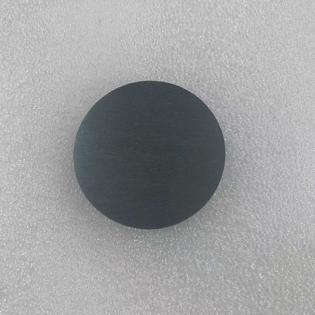
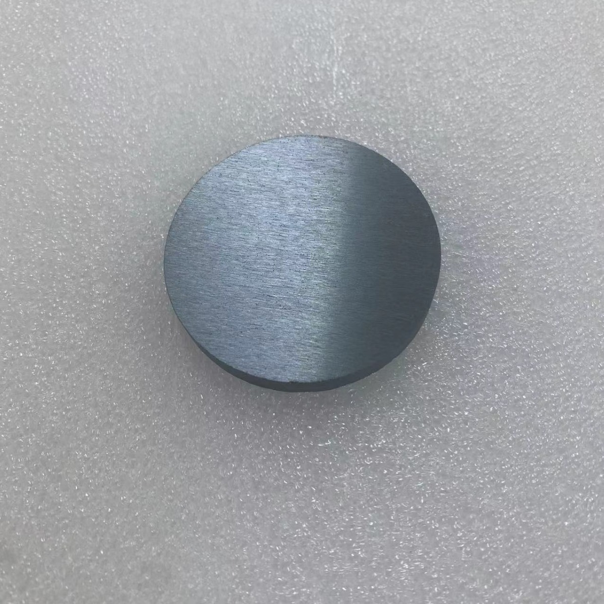
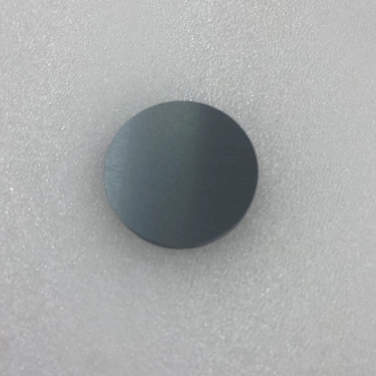
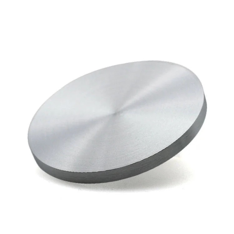
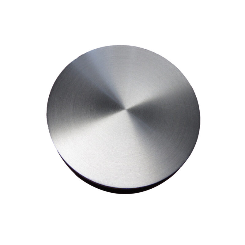
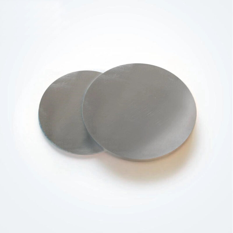
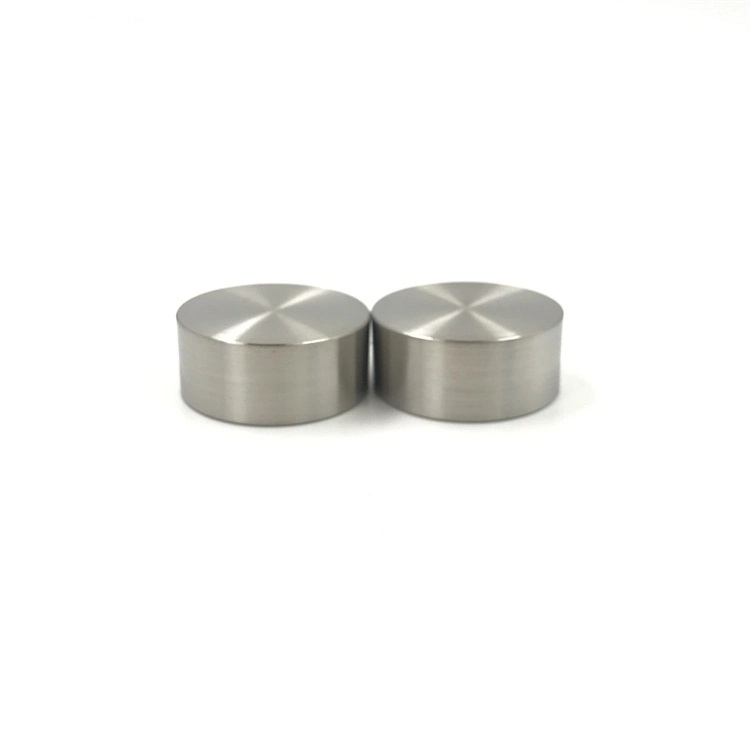
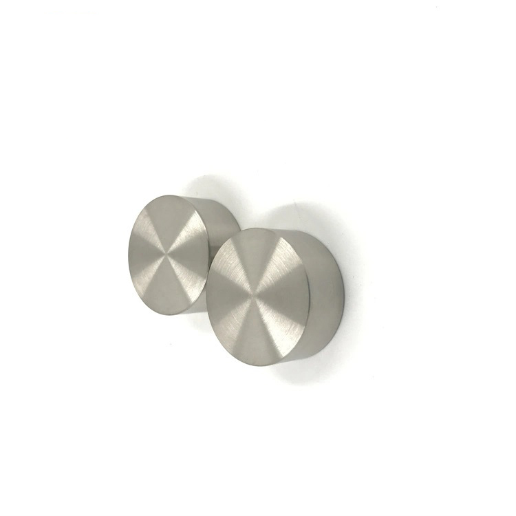
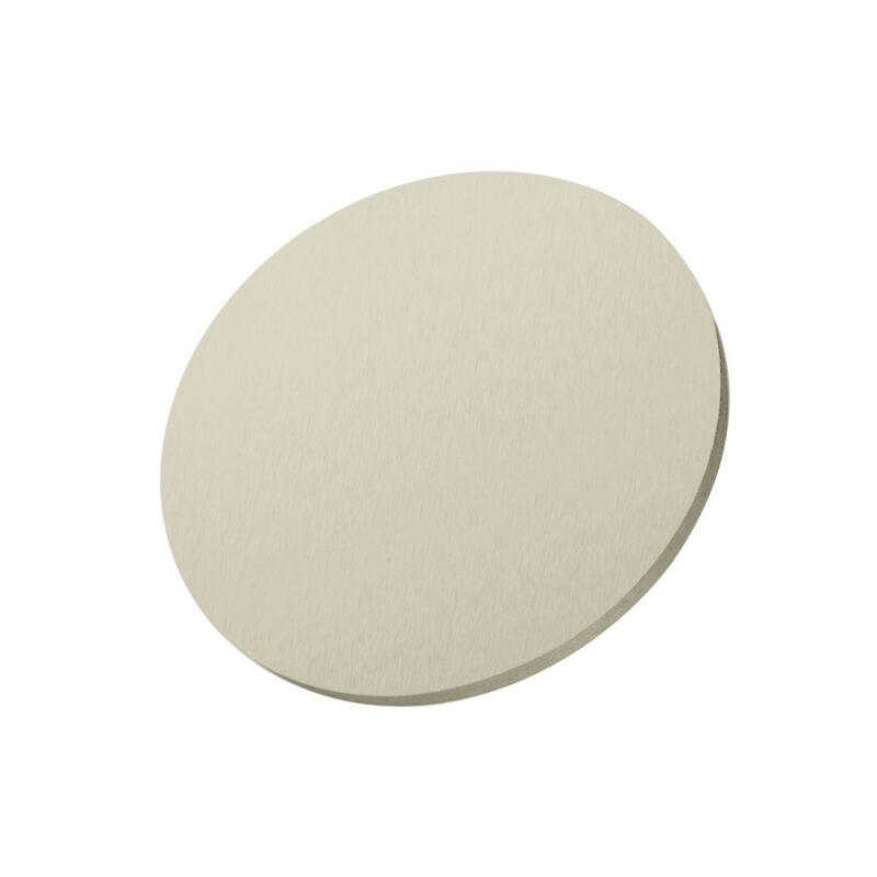
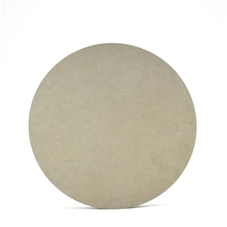
Se Selenium Sputtering Targets
- Purity: High-purity selenium (typically 99.9% or higher) ensures the quality of the deposited films and consistent performance.
- Photoconductivity: Selenium is highly photoconductive, making it ideal for optoelectronic and photovoltaic applications.
- Customizable Size and Shape: Selenium sputtering targets are available in different forms, including discs, plates, and custom shapes, to fit a variety of PVD systems.
- Thermal and Electrical Properties: Selenium films offer excellent thermal and electrical properties, crucial for semiconductor and photovoltaic devices.
Custom products or bulk orders, please contact us for competitive pricing!
- Satisfaction Guaranteed
- No Hassle Refunds
- Secure Payments
Description
| Material | Selenium (Se) |
| Purity | 99.9% – 99.99999% / 3N 3N5 4N 4N5 5N 5N5 6N 6N5 7N |
| Shape | disc, plate, sheet, rod, customized |
| Size | can be customized (contact us) |
| Package | vacuum bag or customer’s request |
| Place of Origin | China |
| MOQ | 1pcs |
| Supply Ability | 10000pcs per month |
| Lead Time | Qty: 1-100, Time: 3-10 days
Qty: >100, Time: to be negotiated |
Selenium (Se) sputtering targets are used in physical vapor deposition (PVD) processes to create thin films with unique electrical, photovoltaic, and optical properties. Selenium is a non-metallic element widely utilized in the production of semiconductor materials, solar cells, and other advanced technologies.
Key Applications:
- Photovoltaics: Selenium is a key material in thin-film solar cells, particularly in CIGS (Copper Indium Gallium Selenide) solar cells, which offer high efficiency in converting sunlight to electricity.
- Semiconductors: Selenium is used in semiconducting thin films for its excellent photoconductive properties, making it ideal for devices such as photodetectors and rectifiers.
- Optical Coatings: Selenium films are applied in optical devices, including sensors and imaging systems, where precise light absorption and transmission are required.
- X-Ray Detectors: Selenium’s high atomic number makes it valuable for use in X-ray detectors, where it helps improve imaging resolution and efficiency.
- Alloying and Coatings: Selenium is used in thin films for its ability to alloy with metals, improving properties such as conductivity and corrosion resistance in various coatings.
Features of Selenium Sputtering Targets:
- Purity: High-purity selenium (typically 99.9% or higher) ensures the quality of the deposited films and consistent performance.
- Photoconductivity: Selenium is highly photoconductive, making it ideal for optoelectronic and photovoltaic applications.
- Customizable Size and Shape: Selenium sputtering targets are available in different forms, including discs, plates, and custom shapes, to fit a variety of PVD systems.
- Thermal and Electrical Properties: Selenium films offer excellent thermal and electrical properties, crucial for semiconductor and photovoltaic devices.
Customization Options:
- Dimensions: Selenium sputtering targets can be tailored to specific requirements, including diameter, thickness, and shape.
- Purity Levels: Available in various purity grades, typically 99.9% or higher, depending on the application.
- Backing Plates: Optional backing plates can be provided for easier installation and improved durability during sputtering.
Selenium sputtering targets from Tinsan Materials offer high-purity Se for thin film deposition, photovoltaics, semiconductors, and optical applications. Custom sizes and shapes available for optimized PVD processes.
If you have specific requirements, such as dimensions, purity, or application details, please contact us to match your needs.
