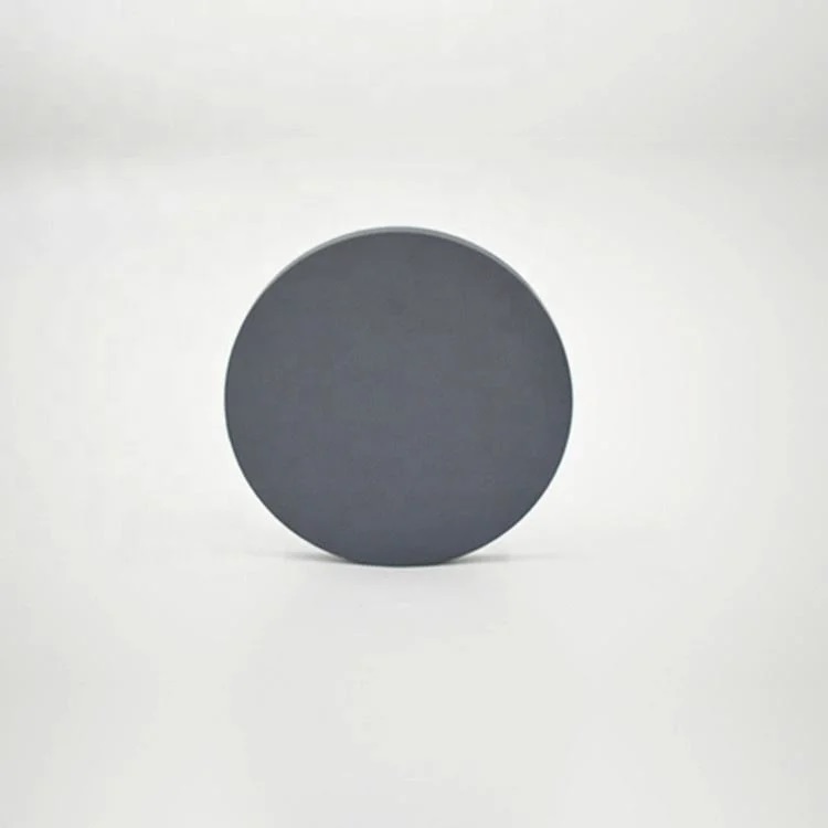
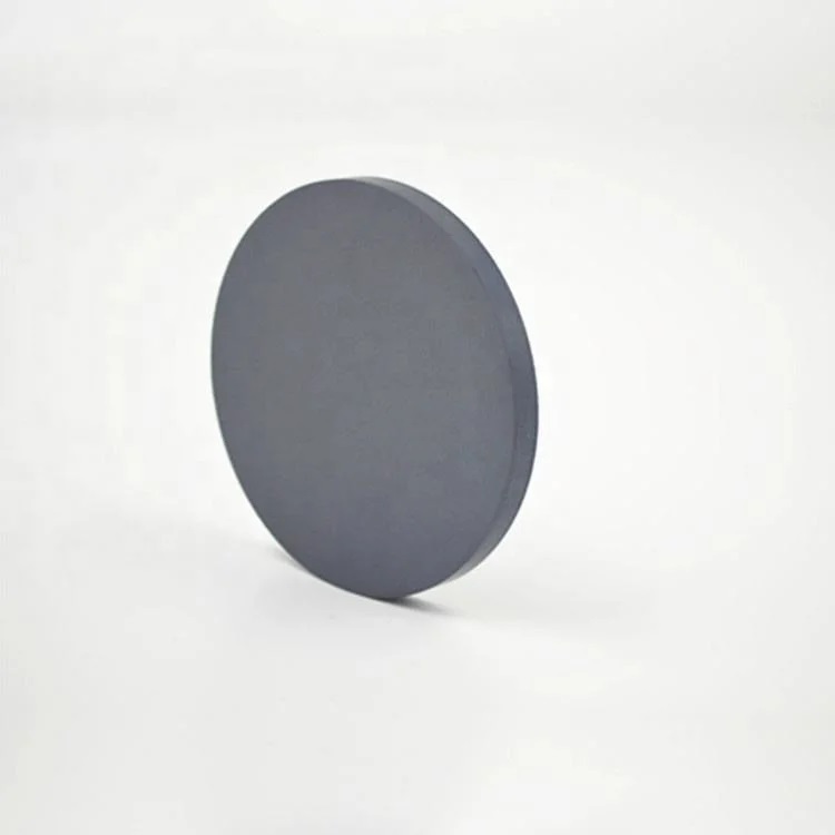
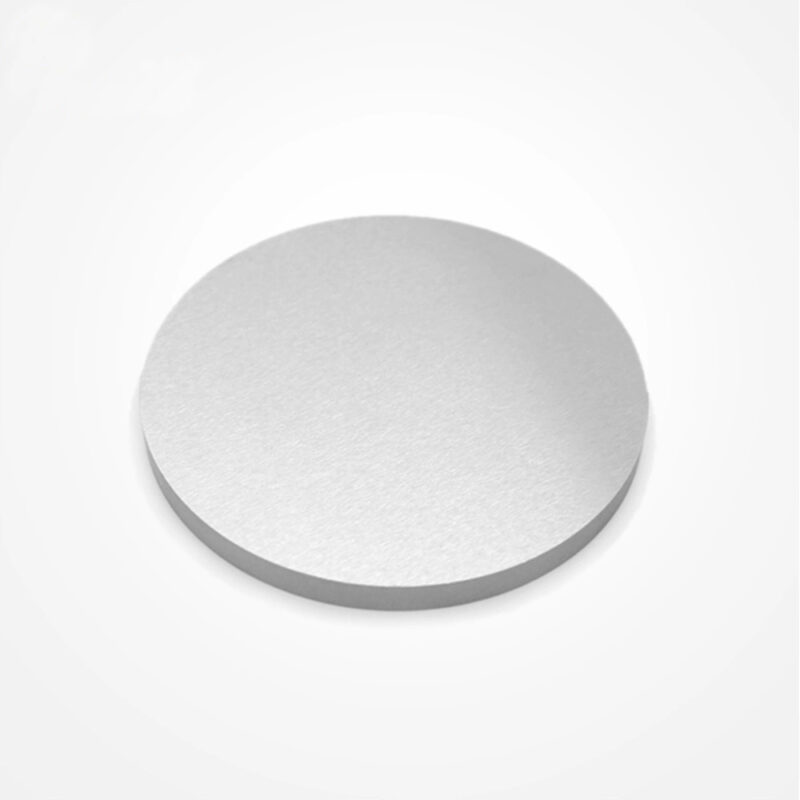
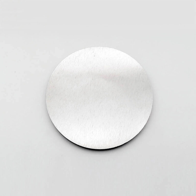
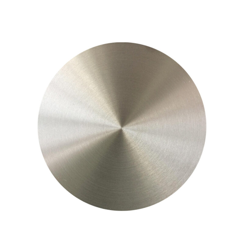
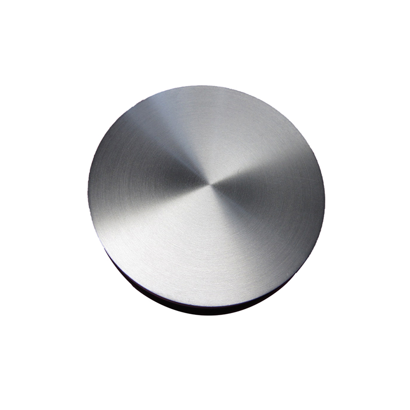
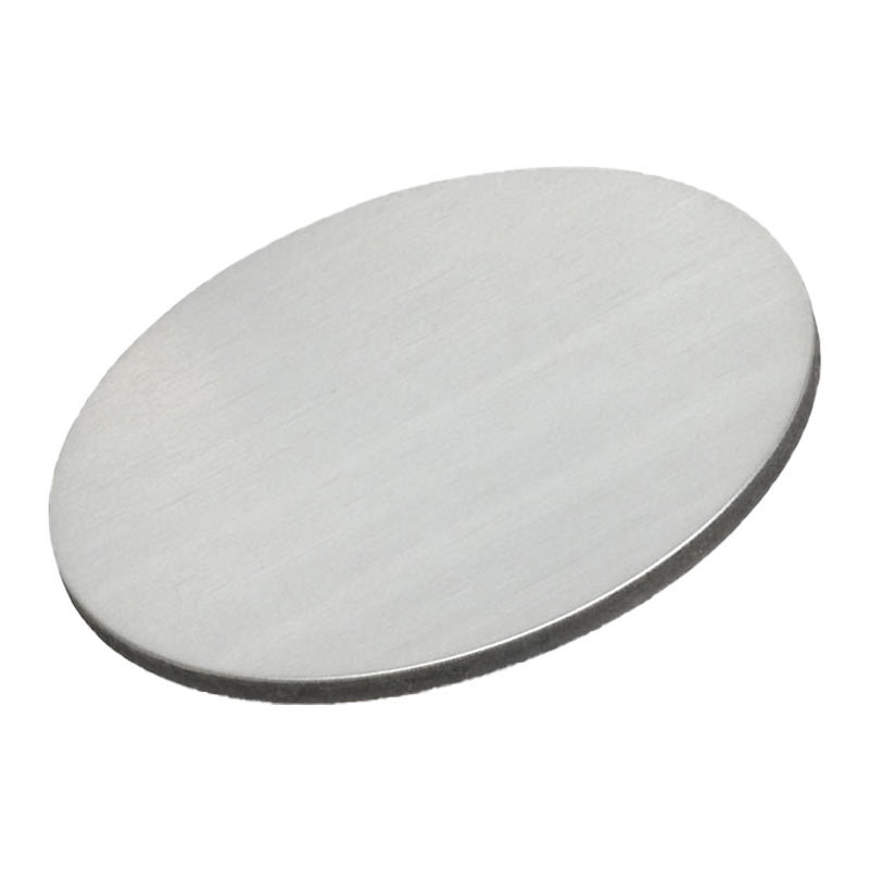
SiO2 (Silicon Dioxide) Sputtering Targets
- Excellent Insulator: SiO₂ has a high dielectric strength, making it a perfect insulating material for electronic devices and integrated circuits.
- High Optical Transparency: SiO₂ is highly transparent in the UV, visible, and near-IR regions, making it suitable for optical coatings and protective layers.
- Chemical Stability: SiO₂ exhibits strong chemical resistance, ensuring that deposited films are durable and stable under harsh environmental conditions.
- Thermal Stability: Silicon Dioxide can withstand high temperatures, making it reliable for use in applications that involve thermal stress.
- Hardness: SiO₂ provides a protective layer that is scratch-resistant and durable, making it ideal for surface coatings.
Custom products or bulk orders, please contact us for competitive pricing!
- Satisfaction Guaranteed
- No Hassle Refunds
- Secure Payments
Description
| Material | SiO2 |
| Purity | 99.9% – 99.99999% / 3N 3N5 4N 4N5 5N 5N5 6N 6N5 7N |
| Shape | disc, plate, sheet, rod, customized |
| Size | can be customized (contact us) |
| Package | vacuum bag or customer’s request |
| Place of Origin | China |
| MOQ | 1pcs |
| Supply Ability | 10000pcs per month |
| Lead Time | Qty: 1-100, Time: 3-10 days
Qty: >100, Time: to be negotiated |
SiO₂ (Silicon Dioxide) sputtering targets are widely used in thin-film deposition processes, especially for optical coatings, semiconductor devices, and dielectric layers. Silicon Dioxide, commonly known as silica, is a ceramic material with excellent insulating properties, making it ideal for applications in microelectronics and optics.
Key Applications:
- Semiconductor Industry: SiO₂ is extensively used as an insulating layer in integrated circuits (ICs) and microchips due to its excellent dielectric properties.
- Optical Coatings: SiO₂ thin films are applied in optical devices for anti-reflective coatings, mirror coatings, and protective layers due to their transparency and durability.
- Dielectric Layers: In thin-film capacitors and other electronic devices, SiO₂ serves as a high-quality dielectric material, contributing to device efficiency.
- Solar Panels: SiO₂ is used in photovoltaic applications for passivation layers, helping to improve the efficiency of solar cells by reducing recombination of charge carriers.
- Protective Coatings: SiO₂ films are often used as protective barriers against environmental factors like moisture, chemicals, and abrasion in various electronic and optical devices.
Features of SiO₂ Sputtering Targets:
- Excellent Insulator: SiO₂ has a high dielectric strength, making it a perfect insulating material for electronic devices and integrated circuits.
- High Optical Transparency: SiO₂ is highly transparent in the UV, visible, and near-IR regions, making it suitable for optical coatings and protective layers.
- Chemical Stability: SiO₂ exhibits strong chemical resistance, ensuring that deposited films are durable and stable under harsh environmental conditions.
- Thermal Stability: Silicon Dioxide can withstand high temperatures, making it reliable for use in applications that involve thermal stress.
- Hardness: SiO₂ provides a protective layer that is scratch-resistant and durable, making it ideal for surface coatings.
Customization Options:
- Dimensions: SiO₂ sputtering targets are available in a variety of shapes and sizes (discs, plates, and custom geometries) for use in different sputtering systems.
- Purity Levels: High-purity SiO₂ sputtering targets (up to 99.999%) are available for use in high-precision applications in optics, semiconductors, and microelectronics.
- Doping: Custom doping of SiO₂ with other elements (such as phosphorus or boron) can be done to adjust the electrical and optical properties for specific applications.
SiO₂ sputtering targets from Tinsan Materials provide high dielectric strength, optical transparency, and chemical stability for thin-film deposition in semiconductors, optical coatings, and protective layers. Custom sizes and high-purity targets available.
If you have specific requirements, such as dimensions, purity, or application details, please contact us to match your needs.
