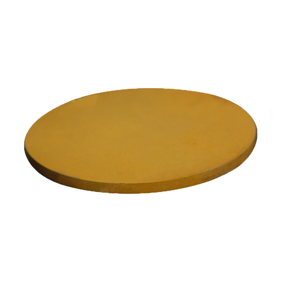
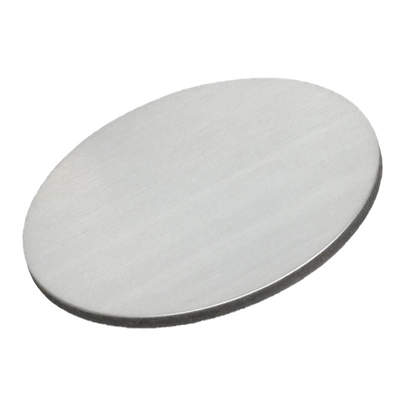
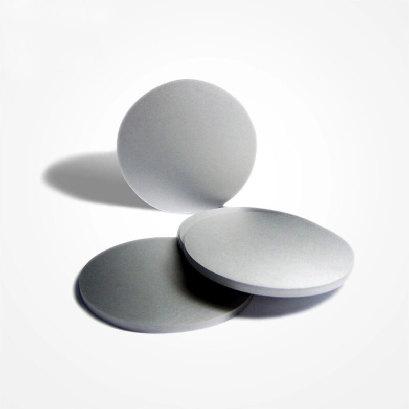
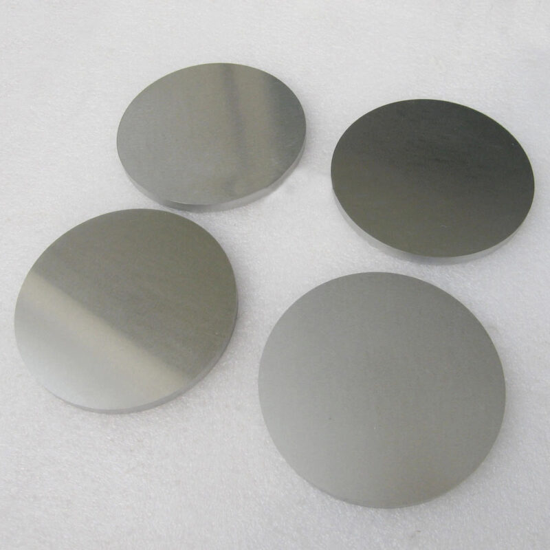
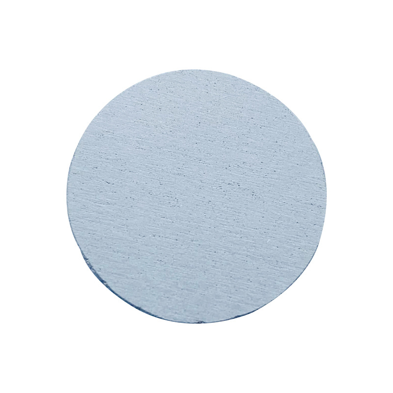
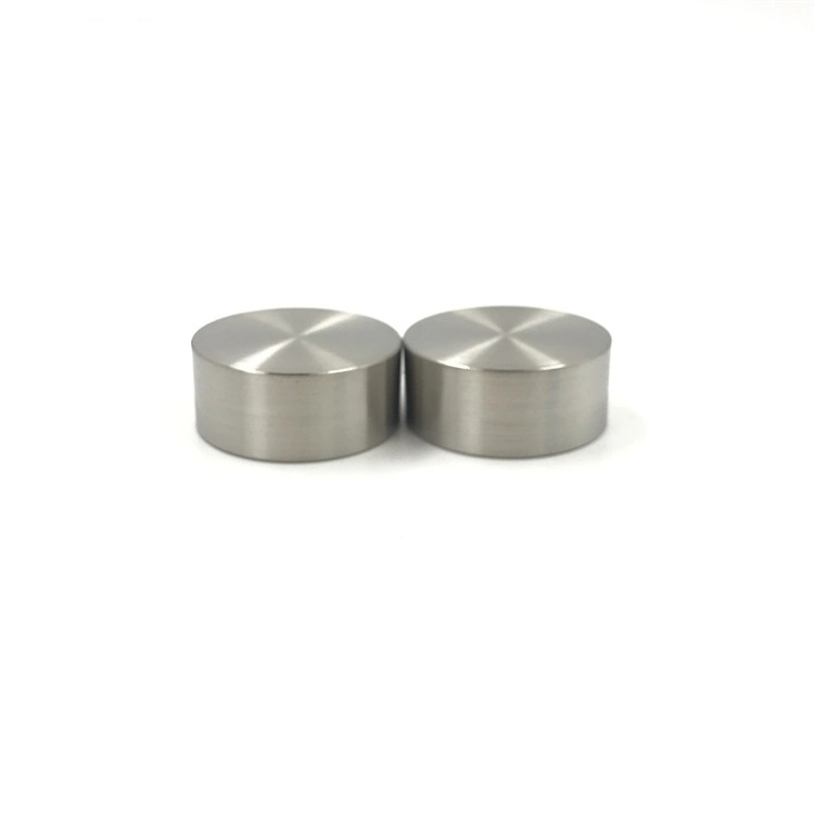
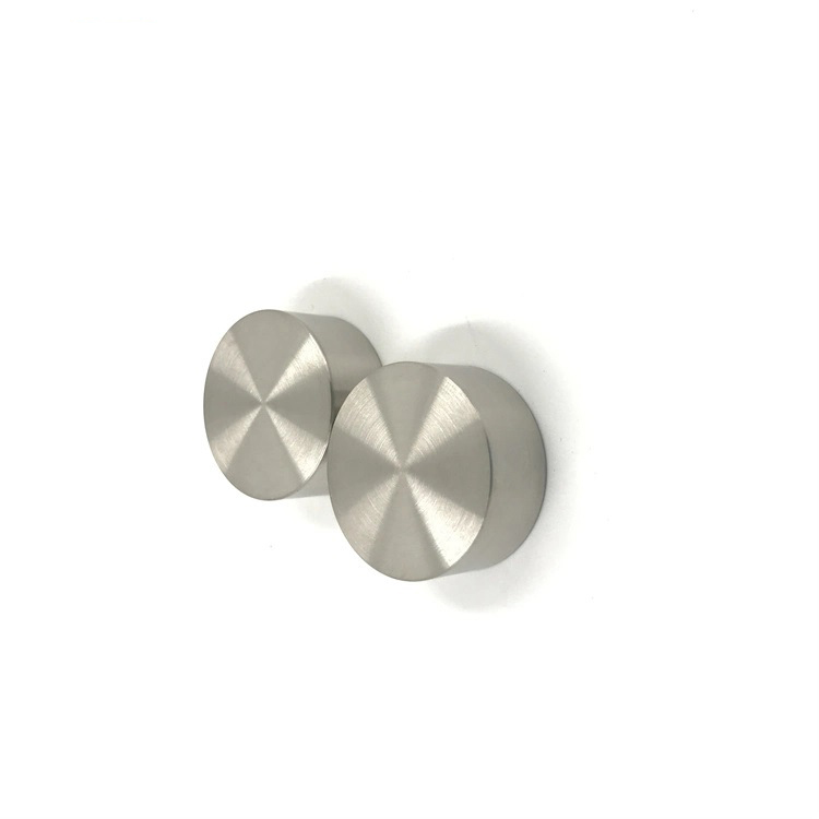
SnS2 (Tin Disulfide) Sputtering Target
- Semiconductor Properties: SnS₂ has a direct bandgap, making it suitable for absorbing light and generating charge carriers, ideal for photovoltaic and optoelectronic applications.
- High Absorption Coefficient: SnS₂ thin films exhibit high optical absorption, making them effective in solar energy harvesting applications.
- Environmentally Friendly: Tin and sulfur are abundant and non-toxic elements, making SnS₂ a more environmentally benign material compared to some other semiconductor compounds.
- Layered Structure: The layered crystal structure of SnS₂ allows for good ion intercalation in energy storage devices and provides opportunities for 2D material applications.
Custom products or bulk orders, please contact us for competitive pricing!
- Satisfaction Guaranteed
- No Hassle Refunds
- Secure Payments
Description
| Material | SnS2 |
| Purity | 99.9% – 99.9999% / 3N 3N5 4N 4N5 5N 5N5 6N |
| Shape | disc, plate, sheet, rod, customized |
| Size | can be customized (contact us) |
| Package | vacuum bag or customer’s request |
| Place of Origin | China |
| MOQ | 1pcs |
| Supply Ability | 10000pcs per month |
| Lead Time | Qty: 1-100, Time: 3-10 days
Qty: >100, Time: to be negotiated |
Tin Disulfide (SnS₂) sputtering targets are used in the deposition of thin films, particularly for applications in photovoltaics, optoelectronics, and energy storage devices. SnS₂ is a semiconductor material with a layered structure and excellent optical and electrical properties, making it suitable for use in next-generation solar cells, thin-film transistors (TFTs), and sensors.
Key Applications:
- Photovoltaics: SnS₂ is used in the fabrication of solar cells due to its favorable bandgap and high absorption coefficient. It is a promising material for thin-film solar cells that aim to be cost-effective and environmentally friendly.
- Optoelectronics: SnS₂ thin films are applied in optoelectronic devices such as photodetectors and light-emitting diodes (LEDs), thanks to their good photoresponsivity and electrical characteristics.
- Energy Storage: SnS₂ is explored as an anode material in lithium-ion batteries due to its high theoretical capacity and layered structure, which allows for good ion intercalation and storage.
- Thin-Film Transistors (TFTs): In electronics, SnS₂ films are utilized in thin-film transistors due to their good semiconducting properties, making them suitable for displays and flexible electronics.
Features of SnS₂ Sputtering Targets:
- Semiconductor Properties: SnS₂ has a direct bandgap, making it suitable for absorbing light and generating charge carriers, ideal for photovoltaic and optoelectronic applications.
- High Absorption Coefficient: SnS₂ thin films exhibit high optical absorption, making them effective in solar energy harvesting applications.
- Environmentally Friendly: Tin and sulfur are abundant and non-toxic elements, making SnS₂ a more environmentally benign material compared to some other semiconductor compounds.
- Layered Structure: The layered crystal structure of SnS₂ allows for good ion intercalation in energy storage devices and provides opportunities for 2D material applications.
Customization Options:
- Target Sizes: SnS₂ sputtering targets can be produced in various sizes and geometries, including circular, rectangular, or custom shapes, to accommodate different sputtering systems.
- Purity Levels: High-purity SnS₂ targets can be manufactured for applications that require precise material quality, such as in the semiconductor industry.
- Bonding Services: For improved thermal management during the sputtering process, SnS₂ targets can be bonded to backing plates to enhance performance and longevity.
SnS₂ (Tin Disulfide) sputtering targets from Tinsan Materials are ideal for thin-film applications in photovoltaics, optoelectronics, and energy storage devices. Offering customizable sizes and high-purity options, SnS₂ targets provide excellent semiconductor properties, high absorption, and environmentally friendly performance.
If you have specific requirements, such as dimensions, purity, or application details, please contact us to match your needs.
